Continue to Site

Welcome to our site!

Electro Tech is an online community (with over 170,000 members) who enjoy talking about and building electronic circuits, projects and gadgets. To participate you need to register. Registration is free. Click here to register now.

  • Welcome to our site! Electro Tech is an online community (with over 170,000 members) who enjoy talking about and building electronic circuits, projects and gadgets. To participate you need to register. Registration is free. Click here to register now.

High gain inverting amplifier problems - please help!

Status
Not open for further replies.

random77

New Member
Hi all,

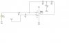
I'm trying to design a high-gain inverting amplifier with a T-network of resistors (see first attachment)

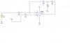
When I built this circuit and tested it separately with a signal generator (5 kHz sinusoid, 2.5V DC offset) it output a massively clipped sinusoid (pretty much a square wave). So i assumed it works as expected. However, when I placed it after the non-inverting amplifier I built before it which works perfectly fine, (2nd attachment) it didn't amplify the input signal at all. In fact it appeared like it attenuated the signal.

The only difference between the signal I used for testing and the one that's used for the design is that the design signal has a bit of noise added to it that will eventually be filtered. Is there something I have to include in this design to make sure it can amplify the signal succesfully? Or is there a connection issue that I haven't taken into consideration? Please help!

Thanks!
 

Attachments

  • High gain Inverting Amplifier.JPG
    High gain Inverting Amplifier.JPG
    46.9 KB · Views: 289
  • Noninverting amp.JPG
    Noninverting amp.JPG
    24.1 KB · Views: 355
So is it fairly safe to assume that nothing appears to be wrong with the design as such? I've only built the amplifier on a breadboard so I don't know if that makes a difference, but if it's all ok, it'll end up on a PCB.

Just FYI, the gain of the amplifier is approximately 1000 and the resistor connected to the positive terminal is to minimize the input bias current errors.

I've found this pdf explaining the amplifier a bit - See page 6 of the attached file.

Hopefully that helps!
 

Attachments

  • High gain inverting amplifier info.pdf
    78 KB · Views: 268
Part of the problem stems from the design as shown in your attachments. The other part of the problem may come from an overdriven configuration with too low a supply voltage. I'll get back to this tomorrow with simulations of your configuration displaying the limitations and another displaying an alternative. Could you please note the value of Vcc and the maximum input drive level. Right now it's late and I need to hit the hay :).
 
The value for Vcc that I'm using is 5V and the maximum input drive current will be no more than 10mA. (I actually measured the current the total current be ~0.6mA but there are other components in my circuit which weren't connected at the time) The reason why I used this configuration in the first place was because to get a gain of 1000 out of standard non-inverting or inverting amplifier will require resistor ratios of 1000 (e.g. 100kΩ and 100Ω).

I'm not saying it's not possible to do to implement this, but from a design perspective I've read from a variety of sources that it's advisable to keep the values of resistors to be close to each other and within the range of 100kΩ and 1kΩ in op amp circuits. This configuration allows me to achieve that but it's being a real bugger to implement properly. :S

I know another option is to split the amplification up into more stages but that will require me to use another chip on my PCB which I want to try to avoid.

Cheers
 
Hi,

I've come across another problem - input bias currents aren't really being minimized and DC offset is about 0.5V. To minimize it, do you have to make sure that the resistance seen in the positive terminal of the opamp is the same as effective feedback resistance? (i.e. (R3||R4||R5) = R2 = 1k (approximately) - see attached file)

Thanks!
 

Attachments

  • High gain Inverting Amplifier.JPG
    High gain Inverting Amplifier.JPG
    18.8 KB · Views: 189
Hi,

I've come across another problem - input bias currents aren't really being minimized and DC offset is about 0.5V. To minimize it, do you have to make sure that the resistance seen in the positive terminal of the opamp is the same as effective feedback resistance? (i.e. (R3||R4||R5) = R2 = 1k (approximately) - see attached file)

Thanks!

I was about to post back to your querys and information. Now I will have to incorporate this additional question into my response. In the mean time you might look up the implications of implementing a high impedence source, vice a low impedence source for various means. My coming response to the initial questions will cover that issue with your design so it would be great if you had some general understanding of source impedance impacts.

EDIT: I have a feeling you created the 2.5V, Vcc/2, in your initial schematic from a simple voltage divider. Am I correct in that assumption? If so, you may see the purpose of my paragraph above.

Merv
 
Last edited:
That's correct - I'll take a look at what you suggested. I think I can see where you're going with this.

Thanks
 
Hi again,

I looked over the inverting stage again and confirmed my thoughts of the other night. The 2.5V pseudo ground you show on your schematic (Vcc/2) has the same label for two very different points indicating a common point and the cause of the problem you experienced; one on the non-inverting input and the other in the feedback loop. These points are not common to the op amp operation if of high impedance (Z), and should not be mingled in that case. Below I'll provide one simulation with your design with one amp showing the commonality of the source with high Z, another with separate high Z sources and a third with a single low Z source and the graphic results for of all three. The maximum input for that configuration with that gain before clipping is about an impractical 35uV, the input level used in the sim; it may work in a sim but probably not in the real world.

Look closely at the top two plots. Note that the signal at PG1, which should not be in the feedback loop at all, is 180 deg out of phase with the output. I'll let you think about that implication and determine the impact on the output and why V(outa) is degenerated to almost nil.

Also, when I asked for the input drive level above I wanted to know what the AC input voltage to the first amplifier to bring into focus the full scope of the issues you were experiencing. Working backwards, I have given you the input limitations for the two different configurations shown below.

The schematics you attached above showed a total gain of over 5800 when coupled together and in an operational configuration, yet you say in your post #2 you expected a gain of 1000. I have included a third simulation of the circuit with the objective, for which I think you are shooting...gain=1000. Also, note with a single-ended supply of only 5V the maximum input level before clipping is ~2mv peak or 1.41mv rms.

One last thing...I used the MC33078 in the sims as that is what I had in my library. The LM833 in your schematics is a clone of the MC33078 in all major aspects of performance so it's apples and apples in that respect.

I feel like I have left something out/hanging, so if you have other questions or need clarification of my comments, please ask so they may be cleared up.

Good luck with your project,

Merv
 

Attachments

  • Three Amps.jpg
    Three Amps.jpg
    126.6 KB · Views: 163
  • Three Amps Plot.jpg
    Three Amps Plot.jpg
    199.8 KB · Views: 154
  • Three Amps with plot.jpg
    Three Amps with plot.jpg
    184.6 KB · Views: 165
Last edited:
Hi Merv,

Thank you very much for that info - that helped me realise that I have to split up the 2 bias points on my bandpass filter as well.

Just to let you know, I'm not actually concerned with whether the input signal becomes clipped or not after amplification as it essentially operates using on-off keying. (i.e. the two signals I receive are either nothing or a ~5kHz signal) Also the signal varies in amplitude depending on how far the transmitter is away from the receiver, but realistic distances for our application is anywhere from 5cm to 1m. So I want to ensure that the signal can be detected reliably from 1m, and hence need the required amplification for that. (I'm under the assumption that because the input signal to the first stage is never going to be above or below the supplies for the opamp that no limiting circuit is required for any stage if clipping is not an issue)

Thanks for all your help once again.

You quite welcome. However, for future reference, it would be very helpful for respondents to your questions if you included all information and full schematics pertaining to the topic up front rather than disclosing such at the end of the discourse. It would save much time and guess work for those trying to help with the issues one has encountered.

Cheers,
Merv
 
Status
Not open for further replies.

Latest threads

New Articles From Microcontroller Tips

Back
Top