Continue to Site

Welcome to our site!

Electro Tech is an online community (with over 170,000 members) who enjoy talking about and building electronic circuits, projects and gadgets. To participate you need to register. Registration is free. Click here to register now.

  • Welcome to our site! Electro Tech is an online community (with over 170,000 members) who enjoy talking about and building electronic circuits, projects and gadgets. To participate you need to register. Registration is free. Click here to register now.

High current PCBs

Status
Not open for further replies.

dknguyen

Well-Known Member
Most Helpful Member
I think I asked this before a year ago but I don't remember anymore (and have some slightly new problems).

How do people pass motor-level currents (~50A) on a PCB? Some of the RC ESCs are tiny and they pass a huge amount of amps. Granted they use huge arrays of MOSFETs so they have large areas of copper, but still...some of these pass 100A.

I was told to solder wire onto the PCB, but the problem is the current still passes through the PCB between where the wire is soldered and the component pad since I can't solder them right on top of each other due to spacing (plus it's really messy even if I could).

I could get 8oz boards made fairly cheaply...the catch is that I'd need to get 155 square inches of it made. Costs $~320 so it's pretty good, but that works out to be 10-20 boards. And they have to be double-sided to have this much copper so it's not like I can route the needed logic circuits onto it as well and panelize it all.
 
resistance is dependent on the length of the conductor. the odd few mils between where your high current trace ends and the pad begins will have a very very low resistance, even if it is 'small' compared to the power trace.

your commercial speed controllers probably use multi-layered PCBs, so they can have one plan dedicated to ground, one dedicated to supply current and another to feed the outputs, with a fourth layer left over for the logic signals.
 
I also vote multilayer. Take care to calculate voltage drops and temperature rises (esp on inner layers) for those high current traces. 50A-100A is doable especially on insane 8oz cu.
 
They don't use PCBs, they use bus bar and MOSFET/IBGBT modules for high currents.
 
The commercial, high-current controllers I have use short traces and have lots of solder on them. It looks almost like they are dipped and is definitely more than one sees with simple plating.

I use 4-oz copper PCB for my homemade ones. For the highest current ones, I use 0.025 copper sheet. The high-current traces are usually pretty simple, so cutting out the traces with a miniature table saw (carbide blade) or scroll saw (jewler's blade) is not too difficult. Hand snips cause too much curling for my taste. A stationary shear would probably work, however. John
 
justDIY said:
resistance is dependent on the length of the conductor. the odd few mils between where your high current trace ends and the pad begins will have a very very low resistance, even if it is 'small' compared to the power trace.

your commercial speed controllers probably use multi-layered PCBs, so they can have one plan dedicated to ground, one dedicated to supply current and another to feed the outputs, with a fourth layer left over for the logic signals.

Actually, that's something that's been bugging me...
a really short trace has realy low resistance, but doesn't it also have much lower heat dissipation? So it generates less heat, but its harder to get rid of the heat so it heats up more? Or is this something here the heat generated scales much faster than the heat the trace is able to dissipate? At the very least, it would seem that the heat generated and dissipated per unit area always remains the same.

janpanhalt said:
The commercial, high-current controllers I have use short traces and have lots of solder on them. It looks almost like they are dipped and is definitely more than one sees with simple plating.

Hmmm. Good point. It never occured to me to just drench the wire end, the component lead, and the pad between them in a thick layer of solder to increase it's current capacity. That's let me use cheaper PCBs...well not cheaper PCBs, the unit cost would be twice as much as it is now, but I'd only get what I need so the total cost is less.
 
Last edited:
I have several halogen lamp driver PCB's I have done at work. Some of them run 25 or more 12 volt, 20 Watt lamps. I just have the soldermask omitted on the drain and source traces for the FET's, make the traces as large as possible, then reflow them with solder during assembly. You can get really large densities and circular mil areas on tracks well reflowed.

I have 50% 1sec on -1 sec off duty cycles at 500 Watts minimum on these boards, no problem. Figure the inrush to the halogen lamps, and the average current is very high. Barely perceptable heatrise on the traces.

Position FETs in a row, do the D trace topside, go wide as posible enveloping the gate, do the S trace bottom side, and spread outward, wide as possible, gate bottomside.

I only use 2 oz, reflowed.
 
Remember for current carrying, cross sectional area is what matters. Look at how thin a PCB trace is and realize how horrible they really are for carrying current. Even on 2 ounce copper PCB the copper thickness is only .0028 inches (70um) At those currents I wouldn't even bother with PCB traces, just use jumper wire of the appropriate thickness. It will take up less physical space in the end and work better than trying to make a thick PCB trace work. Once you get into that kind of current requirement you're almost better off using copper sheeting with some kind of adhesive to FR4 and just having the copper laminate machined. It's not really practical to etch copper more than 2-4 ounces thick as you'll start actually tunneling underneath the etch resist and leaving a T sort of structure, instead of the imagined solid block of copper trace. Over about 1/4 to 1/2 the depth of the copper in trace width will start causing board failures to occur. If you're only dealing the the high current in small sections then just use jumper wire. The cost of a board with masive copper thickness can go up in a hurry, compared to using a thinner cheaper board and a few jumper wires.
 
Last edited:
If with same dimension, an aluminium wire able to carry more current than copper does.
Might that you should check it out what really is. I don't know much.
I ever heard that a tiny super conductor doesn't care with high level current.
But I never saw it my self.
There are various type of PCB as I know.
 
Blatman Bond said:
If with same dimension, an aluminium wire able to carry more current than copper does.
Might that you should check it out what really is. I don't know much.
I ever heard that a tiny super conductor doesn't care with high level current.
But I never saw it my self.
There are various type of PCB as I know.

It doesnt make sense to say one type of metal can carry more current than another. They all can carry any given amount the same. The difference is how much they heat up due to their differences in resistivity.

Aluminum is not as "good" of a conductor as copper BTW. "good" meaning lower resistivity.
 
Sceadwian said:
Remember for current carrying, cross sectional area is what matters. Look at how thin a PCB trace is and realize how horrible they really are for carrying current. Even on 2 ounce copper PCB the copper thickness is only .0028 inches (70um) At those currents I wouldn't even bother with PCB traces, just use jumper wire of the appropriate thickness. It will take up less physical space in the end and work better than trying to make a thick PCB trace work. Once you get into that kind of current requirement you're almost better off using copper sheeting with some kind of adhesive to FR4 and just having the copper laminate machined. It's not really practical to etch copper more than 2-4 ounces thick as you'll start actually tunneling underneath the etch resist and leaving a T sort of structure, instead of the imagined solid block of copper trace. Over about 1/4 to 1/2 the depth of the copper in trace width will start causing board failures to occur. If you're only dealing the the high current in small sections then just use jumper wire. The cost of a board with masive copper thickness can go up in a hurry, compared to using a thinner cheaper board and a few jumper wires.

Sold on the T-structures and reliability. So if I go with regular 1oz copper, I guess I could just use a regular 4-layer so I could also add on logic (for some reason it never occured to me that I could use wires to carry high currents on a multi-layer board...it was always use wires on a 2 layer board mindset).
 
Optikon said:
It doesnt make sense to say one type of metal can carry more current than another. They all can carry any given amount the same. The difference is how much they heat up due to their differences in resistivity.

Aluminum is not as "good" of a conductor as copper BTW. "good" meaning lower resistivity.

Isn't copper both lower resistance and better thermal dissipation than aluminum? I thought the only advantage of aluminum was that it's doesn't oxidize (and might be easier to work with in some cases).
 
dknguyen said:
Isn't copper both lower resistance and better thermal dissipation than aluminum?
Yes, copper is better at both thermal and electrical conductivity.

dknguyen said:
I thought the only advantage of aluminum was that it's doesn't oxidize (and might be easier to work with in some cases).
Aluminium does oxidise VERY quickly, which is why is is very difficult to solder, as soon as you clean the surface it oxidises again almost instantly.

Beware about having copper and aluminium in direct contact with each other. They are widely separated in the electro-chemical series and will corrode each other very quickly.

JimB
 
dknguyen said:
Isn't copper both lower resistance and better thermal dissipation than aluminum? I thought the only advantage of aluminum was that it's doesn't oxidize (and might be easier to work with in some cases).

Yes, which is why it makes a better conductor for most applications. I think aluminum might be a lower cost material. Some applications may require it due to cost.
 
computer motherboards pass 100A or more very easily. Don't use traces - use copper planes - and minimize the distance that the current must flow through. Two or three layers of 2oz copper can easily handle 100A - make sure you have the same number of layers for the return path as well.
 
OutToLunch said:
computer motherboards pass 100A or more very easily. Don't use traces - use copper planes - and minimize the distance that the current must flow through. Two or three layers of 2oz copper can easily handle 100A - make sure you have the same number of layers for the return path as well.

But doesn't all the current converge at the component lead? That's what I was concerned about using regular thickness, extra wide copper traces.
 
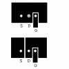
Yes it does converge at the pin, so you maximize track size approaching the pin. This also adds heatsinking, valuable since the PCB conductor shrinks down to the component lead size at the solder point.

This is what I do with TO-220 package FETs, I use 1 oz, and go as large as possible. The Drain is on oneside, the Source on the other. The pad for the Drain is the same shape, just on the other side. If one sided PCBs are used, I do the second image
 

Attachments

  • to220_pcb.GIF
    to220_pcb.GIF
    1.9 KB · Views: 224
Last edited:
THat's a bit more problematic for D2Packs. Oh well, I chose a transistor with a D2PAK-7 where there are 6 source pins and the entire tab is a drain. The PCB trace width calculator says the required width is 2.5" though for 1oz, so I was looking for alternatives to getting 6-8oz PCBs made since I can't use 20 of the same board. I'm starting to lean more heavily towards the wire thing since it would be a LOT easier to route the power traces and gate driver circuits on a single side, and leave the 3 remaining layers for ground, and logic.

The other reason is I haven't decided if I want to push the capacity to 100A since the transistors can handle that, and I doubt the 1oz traces can no matter how wide they are.

THe downside to all this is the feasibility of this project just skyrocketed from where it was before, and if I build this motor driver, then I have to get the $1500 chassis it's going to be used in, build a second duplicate of the driver, build the servo drivers, build the control board...it's a lot of money, but more importantly it's a lot of time I might not have :D:(
 
Last edited:
Status
Not open for further replies.

New Articles From Microcontroller Tips

Back
Top