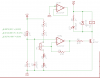
Can someone please tell me why it is necessary to use a 5v+ supply to the pin 10 of the IC1C if the idea is to get 12V+ out of the pin 8? I understand that it is termed as a buffer, but what is it actually buffing? Seems to me that i could just ground the IC1C just like the IC1B & IC1A and feed the pin 8 junction with a 12V+? The V+ is 12v+
Attachments
Last edited: