Continue to Site

Welcome to our site!

Electro Tech is an online community (with over 170,000 members) who enjoy talking about and building electronic circuits, projects and gadgets. To participate you need to register. Registration is free. Click here to register now.

  • Welcome to our site! Electro Tech is an online community (with over 170,000 members) who enjoy talking about and building electronic circuits, projects and gadgets. To participate you need to register. Registration is free. Click here to register now.

Help with non-overlapping clock generator

Status
Not open for further replies.

andrea22

New Member
Hi everyone!
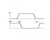
Does anyone know to help me with non overlapping clock generator?
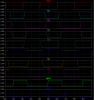
I need to draw how non-overelapping clcks are made?
I tried that but I can't get non-overlapping clocks.
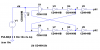
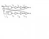
I need to draw signals at the output of each logic gate in this circuit
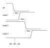
Actually I need timing diagrams for Vin,V1,V2,V3,V4,V5,V6,V7?
Logic gates are realised in CMOS technology and all logic gates have some delay.
 

Attachments

  • generator1.JPG
    generator1.JPG
    17.4 KB · Views: 1,401
Last edited:

Attachments

  • nonoverlapping clock generator sch.PNG
    nonoverlapping clock generator sch.PNG
    16.4 KB · Views: 4,758
  • nonoverlapping clock generator waves.PNG
    nonoverlapping clock generator waves.PNG
    30.3 KB · Views: 1,283
Thank you but I need to draw this circuit on the paper,actaully
I need to explain how non-overlapping clocks are made,so I must
draw that without LTSpice,Pspice...?
What I ment I don't know how much is delay for each logic gate.
 
Last edited:
Thank you but I need to draw this circuit on the paper,actaully
I need to explain how non-overlapping clocks are made,so I must
draw that without LTSpice,Pspice...?
What I ment I don't know how much is delay for each logic gate.
 
Gate delay is a function of the logic family, or if you are designing an IC, the process. For commercially available gates, look up gate delays in datasheets.
 
Last edited:
I think that you don't understand me.I need an explanation why
these clocks are non-overlapped? I don't know what device are used (by type number),
I only know that all logic gates are realised in CMOS technology.
So I don't know how to draw signal at the output of first NAND gate,actually why on the diagram
you were posted rise time and fall time (tphl i tplh are diffrent) of signal V1 are diffrent,but
rise time and fall time at the output of the inverter are the same?
 

Attachments

  • diagrams.JPG
    diagrams.JPG
    12.9 KB · Views: 820
Last edited:
I think that you don't understand me.I need an explanation why
these clocks are non-overlapped? I don't know what device are used (by type number),
I only know that all logic gates are realised in CMOS technology.
So I don't know how to draw signal at the output of first NAND gate,actually why on the diagram
you were posted rise time and fall time (tphl i tplh are diffrent) of signal V1 are diffrent,but
rise time and fall time at the output of the inverter are the same?
NAND gate rise and fall times in this simulation differ by less than a nanosecond. Exact transition times are not very important when analyzing this circuit. Propagation delays are the relevant numbers. The ones shown in the simulation are from models, and may not accurately reflect the datasheet values.
If you were not given part numbers, I would think you could assign arbitrary propagation delay specs, and then analyze the circuit based on these specs. Alternately, pick a logic family, like CD4000, or 74HC, or whatever, and use those specs to analyze the circuit.
My schematic has part numbers. The datasheets of these parts have propagation delay and transition time specs. What else do you need in order to analyze the circuit? Do you know how to analyze the circuit?
 
Last edited:
Well,now I am confused.
Can you help me to analyze the circuit?
I only need to draw that diagrams without using LTSpice,Pspice?
 
Well,now I am confused.
Can you help me to analyze the circuit?
I only need to draw that diagrams without using LTSpice,Pspice?
What did I do to confuse you?
Start the analysis when the clock goes low. Why? Because this will force node 1 low, independent of the other input to U1 (node 7).
Plot nodes 2, 3, and 4.
Calculate node 5.
Plot nodes 5, 6, and 7.
Calculate node 1.
Repeat the process.
 
Last edited:
How can I draw node 2,3,4 without node 1,I don't understand that?
In your simulations pulse width logic 1 of signal V2 is less then pulse width logic 1 of input clock V(clk)?
Can you give me an example?
 
Last edited:
How can I draw node 2,3,4 without node 1,I don't understand that?
In your simulations pulse width logic 1 is less then pulse width logic 1 of input clock?
Can you give me an example?
First, let's agree that Tpd is the value of the propagation delay.
When the clock goes low, node 1 will go high Tpd later. Node 2 will go low Tpd later. Node 3 will go high Tpd later, etc. Just proceed through node 7, which goes back to Q1. You will find that node 7 goes low. This means that node 1 will not change immediately when clk goes high. Q6 WILL be immediately affected when clk goes high. Trace that transition through nodes 5, 6, 7, etc.
 

Attachments

  • timing.PNG
    timing.PNG
    3.6 KB · Views: 468
My questions is:How can you draw V4 on this way?
In last diagrams which you posted nand gate and inverters have same propagation delay?
 
My questions is:How can you draw V4 on this way?
In last diagrams which you posted nand gate and inverters have same propagation delay?
V4 is clk, inverted and delayed by Tpd.
Yes, I used the same Tpd for NAND and inverters, but that was for simplicity. You need to use the Tpd values specified for the devices in your circuit.
 
On that way in your diagrams will be that V4 and V1 are the same signals?
That's not possible.
There I 'm confused.How to draw V4 and V1 on way you posted?
 
On that way in your diagrams will be that V4 and V1 are the same signals?
That's not possible.
There I 'm confused.How to draw V4 and V1 on way you posted?
If Tpd for the NAND and the inverter are identical, V4 and V1 will look the same on the falling edge of clock, but not on the rising edge. You have to follow the process I outlined in post #11, and plot all signals through an entire cycle of clk. Do not try to plot both edges at the same time!
 
Does it mean that I must plot both of edges at the same time only for signal V4,but
for signal V1,V2,V3,V5,V6,V7 must not.
 
Does it mean that I must plot both of edges at the same time only for signal V4,but
for signal V1,V2,V3,V5,V6,V7 must not.
You can plot clk and V4 first, over a couple of cycles if you want, because clk is independent, and V4 is only dependent on clk.
 
I tried everything you said,but I always get overlapped clocks.
I don't where is my mistake.I am desperate.
I can't get non-overlapping clocks.
Can you help me with that,I need that for tomorrow?
 
Last edited:
Status
Not open for further replies.

Latest threads

New Articles From Microcontroller Tips

Back
Top