Continue to Site

Welcome to our site!

Electro Tech is an online community (with over 170,000 members) who enjoy talking about and building electronic circuits, projects and gadgets. To participate you need to register. Registration is free. Click here to register now.

  • Welcome to our site! Electro Tech is an online community (with over 170,000 members) who enjoy talking about and building electronic circuits, projects and gadgets. To participate you need to register. Registration is free. Click here to register now.

Help Me Understand

Status
Not open for further replies.

liinstaller

New Member
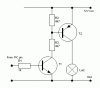
I attached a circuit borrowed from WinPicProg tutorials. Hope they don't mind for an educational purpose.

I understand the basics of how the circuit works but would like to know how to calculate resistor values. I understand how to calculate the values for a single transistor acting as a switch from a PIC but once you throw in a second as in the attachment I become lost. It's not for any particular design so lets just assume that it requires 100mA from T2 and each transistor has a current gain of 50. Also La2 doesn't have to be a lamp.
 

Attachments

  • lamp_source2.gif
    lamp_source2.gif
    2.3 KB · Views: 177
As shown, it is a poor design, primarily due to wasting PIC POWER, and not turning on T2 hard enough.

To turn on T2 hard enough to prevent it from self-heating (i.e. to saturate it), its base current should 1/10th of its collector current. Since its base is at ~0.8V lower than 12V, and the collector of T1 is saturated (~0.1V) above ground, R3= (12-0.8-0.1)/0.01 = 11.1/0.01 = 1110Ω, say a std. value of 1K1.

Now, the collector current of T1 is ~10mA, so its base current when the port pin is high should be about 1mA (to saturate it). If the PIC Vdd is 5V, R1 = (5-0.7)/0.001 = 4K3.

That leaves R2: its function is to make sure that T2 is off when T1 is off. It will never have more than ~0.8V across it, and it shouldn't steal much base current from T2 when T1 is on, say <1% of 10mA, R2 = 0.8/0.1mA = 8k. Actually, the 4K7 that was there originally would work fine...

Stare at a sim of the corrected circuit: Note the base currents of each transistor...

Note that 1mA from the PIC becomes 10mA becomes 100mA at the load.
 

Attachments

  • DF96.png
    DF96.png
    32.6 KB · Views: 171
Last edited:
Yes.
The current gain of a transistor is used when it is a linear amplifier with plenty of collector to emitter voltage. For the transistor to saturate then then it needs a lot more base current than calculated from its current gain. Most transistor datasheets show the maximum saturation voltage loss when the base current is 1/10th the collector current even if the current gain is very high. A few high gain European transistors (BC547) show the base current at 1/20th the collector current.
 
Thanks MikeMl, that was exactly what I was looking for. I just have one quick question about the quote below.

Am I correct in assuming that the ~0.8V and ~0.1V are the Vbe(sat) and Vce(sat) that could be found in a data sheet?

Since its base is at ~0.8V lower than 12V, and the collector of T1 is saturated (~0.1V) above ground...
 
Thanks MikeMl, that was exactly what I was looking for. I just have one quick question about the quote below.

Am I correct in assuming that the ~0.8V and ~0.1V are the Vbe(sat) and Vce(sat) that could be found in a data sheet?

Yes, in principal. However Vbe may not be quoted as Vbe(sat) and it may not be quoted at all as it varies little between transistors. Vce(sat) will probably be quoted, and it also won't vary very much for different transistors at such a small load.
 
Thanks Diver300

Seems like the characteristic curves give the values that are needed. I guess the electrical specification list in the data sheets are only shown for a few values and don't show the whole picture over a variety of currents. I think I'm starting to understand.
 
The curves in a datasheet for a transistor show a "typical" device. But some are worse than typical and the datasheet prints "minimum" specs for them.

If you mass produce a product and design the circuits using "typical" specs then most will work but some will not.
If you design the circuits using "minimum" specs then all passing transistors will work.

I design all my circuits using minimum specs and have never had one that does not work.

Go to the electronics parts store and ask for a transistor that is tested to have typical or better specs. They will laugh at you because you get whatever they have, typical or worse.
 
If you mass produce a product and design the circuits using "typical" specs then most will work but some will not.
If you design the circuits using "minimum" specs then all passing transistors will work.

Do you mind expanding on the "minimum" specs. I attached part of a data sheet for a 2n2907 from ON Semiconductor. I chose that one because I've played with it before. Feel free to use something different if you like.

Any help would be greatly appreciated.
 

Attachments

  • P2N2907A_ON.pdf
    23.8 KB · Views: 137
The "typical" curves on the datasheet of the ON Semi 2N2907A are missing from your attachment. Many people design circuits using the "typical" current gain then find that many circuits don't work because the actual current gain of their transistors is less than the "typical" and is near the minimum value.
The base-emitter voltage of a transistor also has a minimum, typical and maximum value. Then an emitter resistor provides bias stability among many transistors.
 
I understand what you are saying about the min, typ, and max but the question i have is what to do when only a maximum is listed, as the Vbe(sat) and Vce(sat) in the part of the data sheet that I attached in my earlier post? I have seen this in numerous data sheets before.

Thanks again for all the help.
 
I understand what you are saying about the min, typ, and max but the question i have is what to do when only a maximum is listed, as the Vbe(sat) and Vce(sat) in the part of the data sheet that I attached in my earlier post? I have seen this in numerous data sheets before.
You need to look at the worst spec numbers and design the circuit for them to ensure that every passing transistor works, not just the "typical" and better ones. Some specs like current gain have a low number as the worst and some specs like these voltage losses have a high number as the worst.

The Vbe(sat) max and Vce(sat) max are the worst specs (because they show how much voltage loss and how much heat will be produced) then the "typical" specs do not matter. If you design a circuit that works well for these max (sat) specs then a "typical" or better transistor will work even better.
 
Last edited:
The Vbe(sat) max and Vce(sat) max are the worst specs (because they show how much voltage loss and how much heat will be produced) then the "typical" specs do not matter. If you design a circuit that works well for these max (sat) specs then a "typical" or better transistor will work even better.

That clears things up. The confusion was coming from me thinking of "minimum" as the actual minimum and not the worst case specs as you pointed out. Thanks again for the help.
 
Status
Not open for further replies.

Latest threads

New Articles From Microcontroller Tips

Back
Top