Continue to Site

Welcome to our site!

Electro Tech is an online community (with over 170,000 members) who enjoy talking about and building electronic circuits, projects and gadgets. To participate you need to register. Registration is free. Click here to register now.

  • Welcome to our site! Electro Tech is an online community (with over 170,000 members) who enjoy talking about and building electronic circuits, projects and gadgets. To participate you need to register. Registration is free. Click here to register now.

H bridge MOSFET gate

Status
Not open for further replies.

fabbie

New Member
I think i posted this yesterday. seems that this post went missing

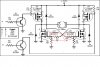
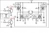
OK looking at the diagram below, the Vgs of the MOSGETS are being supplied with 12V from the power supply.
After reading through some mosfet material, it seems that the mosfet Id and Rds is controlled solely by the Vgs.

I circled the 2 resistors at the N-channel gate. Are they necessary? since the gate is controlled solely by voltage

Thx in advance for any comments :)
 

Attachments

  • mosfetmod1.jpg
    mosfetmod1.jpg
    95.2 KB · Views: 5,181
Purpose of gate resistors in MOSFET circuits are to control the switch-on and off times, and also to help prevent parasitic oscillations
 
Heh. i thought they were current limiting resistors at first. I thought that switch on and off time were already controlled by the 10K resistors across the gate-source junction.
Do the P-channel mosfets require them then?

By the way, what do you mean by parasitic oscillation? does it mean noise?
 
The resistors between the gate and source is to prevent the device from turning on when the gate (high impedance) is not connected to a drive signal (it is a safety precaution and good practice). For high frequency operation these will often be omitted due to the unwanted effects from stray properties

Myself as a rule always put some gate resistor in series, sometimes only a small value (22 -100Ohm) depending on my design (device) and switching frequency.

In your case the values are high because you are operating at DC. If you make the value too high the max gate voltage will be limited by voltage divider action. The same will happen if you make the g-s resistor too low.

Parasitic oscillations, can cause the device to go into high frequency oscillations under certain conditions that can destroy the device due to heat.

https://www.fairchildsemi.com/an/AB/AB-9.pdf

Note that selecting gate resistors, the values are calculated for critical switching applications by using data and not by "rule of thumb"
 
One thing i dont understand is how can gate resistors control the on-off time. werent the rise-time and fall-time already determined by the type of transistor used?. I dont recall there were any equations relating resistance to switching frequency.
:?: :?:
 
fabbie said:
One thing i dont understand is how can gate resistors control the on-off time. werent the rise-time and fall-time already determined by the type of transistor used?. I dont recall there were any equations relating resistance to switching frequency.
:?: :?:

Although FETS are voltage-controlled device just like BJT are current-controlled devices - This isnt entirely true.

For a BJT to start to conduct it MUST have abt 0.6V at its base-emitter.

For a FET something similar is needed. There exists a Gate-Source capacitance.

Sicne as you now there is a gate threshold voltage that needs to be reached before the device starts to conduct. So if you put a series GATE resistor you now have effectively a low-pass filter

So If you increase the gate resistance then it will take longer for the gate capacitance to charge up. If it takes longer for the gate capacitiance to become charged then it will take longer for the FET to start conducting.

You really want the FET's to turn on as fast as possible so use a 10Ohm resistor.

A trick that I use When dealing with H-bridges made from IGBT's and FETS is to use for the gate resistor for each FET a resistor and a resistor-diode in parallel. That way (depending on the orientation of the diode) I can have a slow turn on and a fast turn-off. That way I can stop shoot-through during switching of a H-bridge leg
 
The gate has input capacitance, so a certain current is necessary to charge it up in some time period. If you make the series resistor low it will charge and discharge faster.

Some applications you want very fast switching and others you choose to burn up some energy in the device to reduce voltage spikes caused by leakage inductances at turn off. The faster you turn of the device in this case can produce voltage spikes high enough to exceed the Vds max of the device due to the relation V=L(leakage)*di/dt

where di = change in current, dt = time to turn off

So for example with 1uH of leakage inductance and 10A current change, switching off in 100nS will cause a voltage spike of 100v over your device, which over the Vds rating for your device.

So it is a balance of the amount of energy you will allow the device to burn and the inductive spike your device can handle. With inductive loads the problem is not normally at turn on, as current will ramp up (voltage leads current) due to the inductance reducing the instantaneous power dissipation in the device

As Styx said you can have different on and off times by using another resistor and a diode in the gate circuit.
 
So not what I said then One???


As to the overshoot, true the overshoot is directly related to the switching speed of the FET. BUT it is more related to the matching of the free-wheel diode as well as power-component layout.


To minimise the overshoot. First ensure that the anti-parallel diode is match (in its switching characteristics) to teh MOSFET.

Equally, the stray inductance between the FET's Source and the Diodes kathode (as well as the FET's Drain and the Diodes Anode) Needs to be reduces via the use of decent tracking (preferably via BUS-BARS).

Also DC-link capacitance of suitable value and material also helps


Then and only then look at the voltage overshoot w.r.t. the switching speed of the FETS. In principle the switching speed of the FET needs to be as fast a posible to reduce the switching losses. You will always get an overshoot.

However, the overshoot level w.r.t. the voltage rating of the device as well as the switching speed needs to be examined. If the device is rated as say 1200V and at full current you get an overshoot of 600V I wouldn't be concerned. But 800V and I would then start slowing down the particular device that is havin gthe problem (if no improvement in the power layout can be achived)
 
Styx said:
So not what I said then One???

I was busy typing my response to fabbie in a question to me as part of an on going discussion over several posts. I was unaware of what you posted in the mean time, so may have repeated some of the things you already mentioned by the time of submission. I added EDIT in the last sentence to acknowledge what you posted (apparently) before me after reading your post. No reason to get exited :D we are here to help each other. "TheOne"
 
hehehehe. thanks alot for helping me out. Really envy you guys for having so much knowledge. :cry:

I just want to confirm this. Since the gate resistors play such a crucial role in mosfets, i should also add a resistor at the red circles right?
 

Attachments

  • mosfetmod2.jpg
    mosfetmod2.jpg
    95 KB · Views: 1,743
yup, although the on-state resistance of the BJT that is pullting charge out of the to FET mght be high enough - put one in just in case (low value - 10R).

You might have a problem with your two top FET's. They are being turn off by the 10k resistors and that might be extreamly SLOW. With H-bridges Turn-off MUST be fast adn Turn-on slower

You should always have a resistor at the gate of a FET. Since a capacitor is essentailly a short for AC, when you first pulse a FET's Gate there is nothing to limit the gate current and if you are very unlucky you could burn out the gate

Also if you are also unluck you could set up a pearce oscillator.

always some gate resistance


And also dont be envious of us with our knowledge, believe me it is a curse
 
?? has anyone else noticed that the two lower Fets gates are connected to the motor drive circuitry??
who knows what all that static will do to the overall operation of the circuit??
 
I know!!!

What I dont understand is why he isnt shorting the P-type and the N-type gates together of one H-bridge leg. Then use a NPN-PNP push-pull gate driver per leg
 
prolly - might work for that

well this has convinced me to write a HOWTO on power electeronics for this forum - will take a bit of time but will be done
 
well i dont like the whole design..
even the two upper gate inputs are tied to Vcc throuh a resistor , which will also receive massive spikes when turning on and off..
 
I think the reason it works, is that the motor size may be small so none of the harmful effects are amplified enough to be a real problem.

The original "designer" mention and warns about the "not allowed" state but made no attempt to employ a (easy) lock-out circuit to prevent this :?:
 
:( . can anyone suggest a better h-bridge using mosfet ? im not good enough to design one by myself yet :cry: . i feel demoralised. thx for informing me though of the poor design
 
Status
Not open for further replies.

Latest threads

New Articles From Microcontroller Tips

Back
Top