Continue to Site

Welcome to our site!

Electro Tech is an online community (with over 170,000 members) who enjoy talking about and building electronic circuits, projects and gadgets. To participate you need to register. Registration is free. Click here to register now.

  • Welcome to our site! Electro Tech is an online community (with over 170,000 members) who enjoy talking about and building electronic circuits, projects and gadgets. To participate you need to register. Registration is free. Click here to register now.

Full Bridge Inverter Simulation

Status
Not open for further replies.

Maverickmax

New Member
Hi

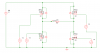
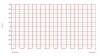
I have been using a SIMetrix simulation for conducting investigation on a simple full bridge inverter. I expect the waveform to be bipolar but I keep getting the unipolar waveform as shown below. I am aware that voltage waveform should be bipolar but it is not happening on my simulation. Please tell where did I go wrong?

Regards

MM
 

Attachments

  • FullBridge_Analysis,jpg.png
    FullBridge_Analysis,jpg.png
    5.9 KB · Views: 2,771
  • FullBridge_Analysis_3-graph.jpg
    FullBridge_Analysis_3-graph.jpg
    94.9 KB · Views: 1,797
Last edited:
Can't tell without more info. What are the voltage output levels and timing of V2 through V4?
 
Can't tell without more info. What are the voltage output levels and timing of V2 through V4?

PWM - 1kHz
Voltage - 200V
Voltage input to each MOSFET - 5V (Offset - 2.5V)
Duty Cycle = 50%
Rise Time = 0 (On every MOSFET)
Fall Time = 0 (On every MOSFET)

Q1 and Q4 - Inverted Square waveform
Q2 and Q3 - Non-inverted Square waveform
 
Last edited:
You cannot drive the gates of upper two FETs WITH RESPECT TO GROUND unless V4 and V5 are +205V!!! (Not a practical way to do it). They have to be driven with respect to their own Sources. Your basic H bridge is not correct.
 
Last edited:
Remember it's the gate-to-source voltage that controlls the transistor, not the gate to ground voltage (unless the source is connected to ground).
 
You cannot drive the gates of upper two FETs WITH RESPECT TO GROUND unless V4 and V5 are +205V!!! (Not a practical way to do it). They have to be driven with respect to their own Sources. Your basic H bridge is not correct.

Please advise me how to proceed it in the correct way?

MM
 
Please advise me how to proceed it in the correct way?

MM
Replace the top two NFETs with PFETs (sources connected to +200V) , and drive the gates of the PFets downward from +200V.
 
Last edited:
Its a trade off!! You can use 4 NFETs and have a horribly-complicated Gate driver for the top two, or you can use PFETs for the top two devices and have a simpler gate driver for the top two; or you can use split -100V and +100V supplies, and have the simplest gate driver...
 
Look up high-side bootstrapped mosfet gate driver. That's what you'll need to drive the upper FETs.
 
You could also use a pulse transformer to control the high side but it will only work for AC voltages and there can't be any net DC e.g. the duty cycle needs to be 50%.
 
You could also use a pulse transformer to control the high side but it will only work for AC voltages and there can't be any net DC e.g. the duty cycle needs to be 50%.
That's true for a DC coupled circuit. But you can use any duty cycle with a transformer if you couple the signal through a series capacitor to keep the average dc current at zero. Of course, the DC level signal at the transformer output will be at whatever is the average value of the signal waveform. From that you likely can use a clamp circuit to restore the DC level to whatever you need.
 
That's sort of true.

The problem is with a very high duty cycle the voltage will be much lower because as you've said the average value has to be zero.
 
Status
Not open for further replies.

Latest threads

New Articles From Microcontroller Tips

Back
Top