Electro Tech is an online community (with over 170,000 members) who enjoy talking about and building electronic circuits, projects and gadgets. To participate you need to register. Registration is free. Click here to register now.
Welcome to our site! Electro Tech is an online community (with over 170,000 members) who enjoy talking about and building electronic circuits, projects and gadgets. To participate you need to register. Registration is free. Click here to register now.
Q1
Yes the expression should be E = F(f0/N - fr).
It could be argued that the /N is wrapped up in the all encompassing F (ie Function of)
Yes the " - " is a minus sign.
Q2
"dc amplifier offset control" sounds like the writer is suffering from verbal diarrhoea.
What he really means is the "dc Error Voltage", ie the output voltage of the error amplifier.
I agree that with your first statement. The output of a phase detector is Fo-Fr, but in this case Fo is really Fo/n.
There are more than one type of phase detector so this depends on what type.
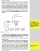
The VCO in this example needs to cover channel 1 to 80 in a range of 0 to 5 volts. I made up 0 to 5V. Channel 40 is about 2.5V. If you change the divide by N to go to a new channel the phase detector will push the DC error voltage up or down to get to the new voltage needed to get no phase error and the right channel. I think this DC offset voltage is the voltage needed to get the right frequency out of the VCO.
Q2: The "DC amplifier offset control" is just the signal E. The "DC amplifier" refers to the fact that this control signal needs to come from a DC amplifier (e.g. OPAMP circuit or something similar). The "offset control" refers to the fact that the VCO outputs a nominal frequency when E=0, and the frequency is offset from nominal as E is offset from zero (not all systems work this way and a DC shift may be needed, which makes the terminology imperfect). This frequency is offset (or tuned) by changing the Voltage E. I'm not sure how universal this nomenclature is, but it is descriptive of the function.
Q2: The "DC amplifier offset control" is just the signal E. The "DC amplifier" refers to the fact that this control signal needs to come from a DC amplifier (e.g. OPAMP circuit or something similar). The "offset control" refers to the fact that the VCO outputs a nominal frequency when E=0, and the frequency is offset from nominal as E is offset from zero (not all systems work this way and a DC shift may be needed, which makes the terminology imperfect). This frequency is offset (or tuned) by changing the Voltage E. I'm not sure how universal this nomenclature is, but it is descriptive of the function.
It's all just terminology that doesn't have too much value. It's probably the same thing, as far as I can tell. I don't deal with PLLs often enough to know if there is a standard nomenclature for that diagram.
For your question, I don't see any reason why it matters which plot is shown above the other. It's just a preference thing as far as I can tell.
The dc_amplifier_offset_control is a somewhat finer detail of the circuit which is mentioned in the text but unfortunately NOT shown on the schematic.
The dc_amplifier_offset_control is responsible for providing an output from the DC amplifier when there is zero output from the low pass filter, as required by the voltage controlled oscillator to provide a nominal output frequency. In many cases this frequency will be around the center of the range of the VCO. Thus, we may see a positive deviation from the nominal output offset or a negative deviation from the nominal output, providing both frequencies above and below the nominal VCO output.
This function may also be relegated to the VCO itself however, or partly so and partly via an actual output offset voltage.
This is probably too detailed for this particular paper anyway, so they didnt want to place too much significance on it and in doing so miss the main points. For example, with a zero offset we dont even have to consider it except to note that it is zero
So they mention it more casually in passing so most people wont worry about it too much for now. In a practical circuit we'd have to think about it of course.
It would have helped if they drew a line showing exactly what part of the circuit the offset was affecting, but again they probably didnt want to focus too much on that little detail. For example, they also didnt draw the power supply leads or bypass capacitors, but we assume they are there and working in a real circuit.
We could argue that is true but then again they didnt actually mention the power supply in the text while they did mention the offset, so this paper was probably written by someone who forgot what it was like to be curious by nature.
The following query is based upon what was said in this post.
For most PIC microcontrollers 10k is the maximum recommended source impedance but the acquisition time can be reduced by reducing the size of source impedance. For instance, this reference gives that maximum acquisition time is 19.72 us when Rs is 10 kOhm (page #428) and minimum acquisition time is 10.61 us when Rs is at its allowed minimum value that is 50 ohm (page #429).
Why does acquisition time increase when source impedance is increased? This is what I initially thought. You can see that only R2 is considered a source impedance and not R1. Here, one thing important to notice that when R2 is changed, R1 should also be changed so that the voltage drop across them doesn't change. If R2 is made 50 ohm then R1 should be 150 ohm. When R2 is decreased (along with R1) the acquisition time decreases because the capacitor C_hold will get charged up quickly because now there is more current flowing thru R1 and R2 to fill it up and pressure across R2 is still the same. The same pressure but more flow. Do I have it correct?
Do you have any idea that why source impedance cannot go lower than 50 ohm? Thank you.
With voltage dividers the problem is that lower resistances will drain current, but higher resistances will provide higher input impedance for ADC. Also, higher resistances increase noise. So, you choose what's more important. It is possible to use higher resistances in the divider and then install a buffer, so that ADC sees low impedance.
This site uses cookies to help personalise content, tailor your experience and to keep you logged in if you register.
By continuing to use this site, you are consenting to our use of cookies.

")