Continue to Site

Welcome to our site!

Electro Tech is an online community (with over 170,000 members) who enjoy talking about and building electronic circuits, projects and gadgets. To participate you need to register. Registration is free. Click here to register now.

  • Welcome to our site! Electro Tech is an online community (with over 170,000 members) who enjoy talking about and building electronic circuits, projects and gadgets. To participate you need to register. Registration is free. Click here to register now.

First homemade PCB (!!)

Status
Not open for further replies.

Blueteeth

Well-Known Member
Hey,

I realise lots of people will post pics of their diy boards but I'm after some constructive criticism.

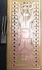
I made this CPLD (TQFP48-0.5mm pitch) - DIP adapter as a real test to see just what toner transfer can do. Materials used:

-Software: Eagle 4.12.

-Printer: Cannon LBP200i @ 600DPI.

-Paper: Stock printer paper. Tried magazines (thick and thin pages), glossy (for inkjet and laser). Every one but the standard cheapo printer paper caused severe smearing/smudging, and the staples photo basic wouldn't even come off after 24 hr's in soak. I'll try proper toner transfer paper (the blue stuff) later.

-Copper clad. Stock SRBP (FR2). Good enough for these circuits, and won't destroy my drill bits after a hundred holes.

-Etchant: Amonium persulphate 100g disolved in 500ml of warm water.

-Drill: Dremel 300, with HSS 0.8 (blunt) and 1.0mm (new) bits. PZ541 drill stand.

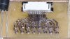
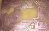
Results? well, considering the pads for the TQFP part were 0.5mm in pitch and 0.34mm wide..thats a gap of 0.16mm. Getting the paper out of these 'trenches' was tough, and meant that three of the gaps did not etch away properly, leaving shorts corrected by a craft knife. Some areas where the toner didn't stick too well were touched up with an etch resist pen. Which was crap and was quickly eaten away by the etchant within minutes.

I think I got the drilling down, despite some off-centre holes, and the ironing seems to require NOT the highest heat as that causes smudging but a pretty high heat, as qwell as a preheated board. But can anyone recommend some decent paper? Preferably stuff that DOESN'T smudge the toner, but comes off without 30 minutes of rubbing and swearing? God knows why people recommend glossy paper, every type I tried results in small pads becoming one large patch of toner.

Suggestions welcome! Next time, I'll try some photoresist, with washing soda as developer :D

Blueteeth
 

Attachments

  • 100_0123.jpg
    100_0123.jpg
    233.2 KB · Views: 1,000
  • 100_0119.jpg
    100_0119.jpg
    378.1 KB · Views: 1,142
Hi Blueteeth,

had similar/worse results trying to use all types of paper/glossy mag paper & etch-resist pen for touching up. Got p****d off trying to remove paper after soaking for ages in warm soapy water, lightly scrubbing with toothbrush, chanting with scented candles etc. and switched to Press 'n Peel...delighted with the results.:D


Good to see you are using a drill press, did you drill the board prior to etching or after? The reason I'm asking is...after etching, the holes left behind will serve to centre the drill bit much better than drilling prior.

Better than my first attempts BTW.
 
Cheers for the response!

Yep I have some p'n'p ppaer, and I'll use it. More expenisve than standard paper, but hey, still gotta be a hell of a lot cheaper than getting lots of one-off small boards made up...as board houses hate one-offs, and I'm not prepared to get 50 adapters for a rare chip that no-one else will want/need.

Yep, I drilled the holes post-etching. You're competely right, not only does the toner help to line up the hnoles by eye,. but the lack of copper also guides the bit. The 'mistakes' on the drilling I would put down to inexperience, lack of light, and a broken 0.8mm drill bit which I found on my desk lol. Did the job, but ripped off pads like theres no tomorrow.

Btw, that little board was part of a larger panel, since I could only make up etchant in 0.5L, was enough for a 100x160mm panel, but not too much to cause hassles with storage (plus, the stuff I use has a shelf life in days rather than weeks). I'll post some pics later once they have been depanelized.

Thanks again, I reckon it was worth experimenting, as I have over 40 projects designed, but no money to get PCB's made, and I hate waiting for things anyway. P&P paper up next, I shall keep you posted.

Blueteeth
 
Last edited:
In Eagle, click on "drill-aid.ulp" It makes the center of pads even smaller and makes drilling even easier after etching. You can make the center any size you want.

John
 
The photo on the left has a lot of lines shorted together and some of the lines look very thin.

The photo on the right is a negative pcb that won't work.
 
That looks good but I'd go down the photo route for something of that higher resolution.
 
My first home made PCB

Hi Scott,

a lot of work taking a close look at the many shorts on the PCB.

This already fine trace technology and asks for different methods.

Here's what I used to do in Germany: Went to a copy & print store (for newspaper advertising and small catalogues), took my Eagle CD with me and installed Eagle on their computer - then loaded the desired file and had a gerber photo plot made on transparent film. The charge for one film was 10€ regardless of its size, so making the board was pretty cheap compared with a professionally made board.

Using UV-resistant raw material (FR4 photolayer by BUNGARD) the board was of superior quality without corrections like carving with a scalpel, very close to the quality of the traces you can see on any mainboard.

To drill the board with holes exactly in the center of the pads I used a BUNGARD drill, a kind of drill press where you have the PCB on a flat table, and a viewing magnifying glas with a grommet underneath for exact positioning. The drill bit worked from underneath the table driven by a solenoid and activated with a foot pedal. This little machine also took care of the dust sucking the board material down the drill hole and from there into a vacuum cleaner. At 60.000 rpm the holes were smooth enough for electrochemical through-contacting.

Using a laser printer with a resolution of at least 1,600dpi (better 2,400) you can achieve similar results provided you use the printer manufacturer's suggested film. Those films have a heat protection paper layer (stick & post method) on one side and don't melt in the laser printer and there is also no distortion in the print.

Kind regards

Hans
 
The photo on the left has a lot of lines shorted together and some of the lines look very thin.

The photo on the right is a negative pcb that won't work.
The OP said there were shorts. He asked for constructive criticism. I think that means offering solutions, if you have them, to problems that you identify.

The photo on the right is correct. The dark areas are toner which will remain after etching. By comparing defects, I would say that both of the photos are of the same workpiece, on the right before etching and on the left after.

I think this was a very good effort, with better results than I've achieved with toner transfer. I still use inkjet transparencies with sensitized boards.
 
I found that the best etch resist pen for me was a black super-fine Sharpie. Although I've never tried an 'official' etch resist pen.
 
For toner transfer I like the PulsarProFx system. The transfer paper is coated with a starch that holds the toner when dry and does a 100% release in about a minute when wet. With this system you never have to remove the transfer medium from between traces and what your printer prints, is what ends up on the PCB.

The transfer paper is now avialable form in England.

The Flightline site will not mention PCBs but the transfer paper they use for graphics is that same used for PCB toner transfer.
 
Last edited:
Hey, Looks like you are having fun making the PCBs and they look good too. I thought I'd just point these out: https://www.futurlec.com/SMD_Adapters.shtml.
It sucks that the pins are on all 4 sides so its not breadboard friendly, but cant really go wrong on the price.
 
Wow, talk about feedback!

Ok, I'll go through the response one by one.

jpanhalt: Cracking idea! I have loads of ULP scripts for eagle, but rarely use them. Having a relatively small 'dot' in the middle of a pad, teoretically *should* centre the drill bit better, as well as easing it into the copper. With my 'standard' holes, by the time the bit had eaten far enough to start taking copper off...it was not so much 'drilling' as 'shearing' meaning tearing pads was quite common. That should sort it out a treat.

audioguru: You're right, the left one did have shorts (only 4 believe it or not), I guess my camera focus/tripod was the best. Sorted it out with a craft knife like a trooper. The right photo...well I thought it was pretty obvious that was 'pre-etch' just to show what the toner was like before etching, perhaps I should have explained it better. The shorts after etching were most likely because of residual paper in the trenches between pads, something press'n'peel should not do.

Hero999 and Bonuk:

Yep, the photo resist method would be far better for finer resolution, and I'm planning on using it for anything under 0.65mm pitch. For soic with 1.27mm or TQFP with 0.65mm this method seems to handle it. This was a test of toner transfer and its limits, as a half-arsed experiment to see if I can contribute something towards it.

Re photoresist... as the presensitized boards are fairly cheap, and with the price of UV LED's dropping, the leap from toner transfer to photo etching shouldn't cost much at all (in theory). As for developer, I don't deal with caustic soda (my pets would find it and drink it) so washing soda (pure sodium carbonate) should do just as well. 54p for 1kg at sainsbury's for all you UK people! I'll have to do a timing test for exposure times. I'm keeping this proper cheap here

Bonuk: I remember using the type of drill you mentioned !! My university had one, and it made drilling 500 holes in my final project a breeze! Alas, until I start making lots of boards, I can't justify the expenditure...that doesn't mean I can't steal ideas from it though... I've already designed/starting making, a plexi guide. Its very similar to the cover found on the drill you mentioned...a single 2mm hole, counter sunk, with a reticle paint on. With that fixed over the PCB, should making lining up those 0.6mm via holes a snap. But I still need to sort out the 'play' in my drill stand, don't think it was designed for a dremel300 (the gastly thing is coated in rubber). Cheers for reminding me about it though!

mneary: Inkjet transparencies? Wow, the other limit I can across was my laser printer. Inkjets have mahoosive resolution, and I wasn't aware you could get transparencies for them? Seems like this photoresist thing is the way to go after all...at least for fine high quality proto's, I'm still digging this toner transfer thing for guitar effects and basic circuits :) The 'etch resist' pen I used, believe it or not, was simple a statler permenant marker. It was sold by rapidonline.com AS an etch resist pen. Guess I should point out to them it was about as resistant as the copper beneath it. Proper ER pens are too expensive. Hmmpf.

3v0: OOo cheers for that link, I have heard of pulsar, but being in the UK, could get hold of it. I'll pick some up once I get paid and give it a whirl.

jrz126: ahh SMT adapters :) I use ebay for them, although futurlec seem to have them even cheaper. I must have at least 60 SMT adapters about, ranging from the usual SOIC8 to PQFP208. The 4-sided ones are always an arse to wire up lol If you would like a list of ebay shops that do SMT adapters (with cheap international shipping) I'd be happy to mesage you? I think for SOIC I could make my own for now. Still, probably worth it for finer pitches, then I can just deal with DIP packages with my PCB's, which this system handles with ease.

Last thing, a couple more pics, one FPC 0.5mm 16 way adapter. And one header board for an LCD controller. Both turned out surprisingly well.

Thanks guys,

Blueteeth
 

Attachments

  • 16SMTFPC05mm.jpg
    16SMTFPC05mm.jpg
    98.9 KB · Views: 306
  • SED1335F.jpg
    SED1335F.jpg
    349.4 KB · Views: 369
Hey blue teeth,

Ive played with a similar method double sided, but I erred on the fatter track larger clearances sided after all electronically this is preferered as it reduces inductance and track impedance
electro-music.com :: View topic - single vs double sided PCB layout would like advise

I have found a great paper the best part is its free!
the Argos catalog yes the laminated book of dreams!
but you want the non laminated ones tape these to an A4 sheet so you dont snag it in the printer then iron it on. It pulls away pretty easy and because its so thin there is less pulp crap to clean up. I tried gloss it was a disaster. Argos paper worked for a pretty dense design without too much distortion. I have the same drill and just bought the stand on other forum recommedations.. What do you think about it? any mods to improve it? the mounting bracket and rack seems to be .1mm play which is not great but probably okay. I had the idea to use a small nail to punch each pad to guide the drill.

good luck

wilson
 
Status
Not open for further replies.

Latest threads

Back
Top