killivolt
Well-Known Member
Ok, thanks to ChrisP58 in another thread, he suggested the possibility of changing a circuit design with a single Primary GDT and offered the Center Tap GDT. He gave me a simple explanation which is understandable, for a guy like me.
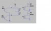
I'm confused about the 12v supply in the image below the first schematic, because SG3525 already has a supply provided through the internals of the Chip?
not sure if this will work in this schematic. Bear in mind I know the diodes would have to be removed, I have thought some descrete Transistors might work and might be needed since SG3525 drivers shouldn't exceed 500ma. I'm just not sure if they would lag or mess the timing up if they could be used. If someone can understand and help me with my quandary's it would greatly appreciated.
Thanks,
kv
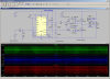
**broken link removed**
ChrisP58,The two NPN transistors are internal to the PWM chip.
When Q1 turns on it will pull A low, B will swing up to +24V, The upper mosfet will see a negative 12V pulse, and the lower mosfet will see a positive 12V pulse. When Q2 turns on, everything swaps state.
I'm confused about the 12v supply in the image below the first schematic, because SG3525 already has a supply provided through the internals of the Chip?
not sure if this will work in this schematic. Bear in mind I know the diodes would have to be removed, I have thought some descrete Transistors might work and might be needed since SG3525 drivers shouldn't exceed 500ma. I'm just not sure if they would lag or mess the timing up if they could be used. If someone can understand and help me with my quandary's it would greatly appreciated.
Thanks,
kv
**broken link removed**
Attachments
Last edited:
") .
.