ThomsCircuit
Well-Known Member
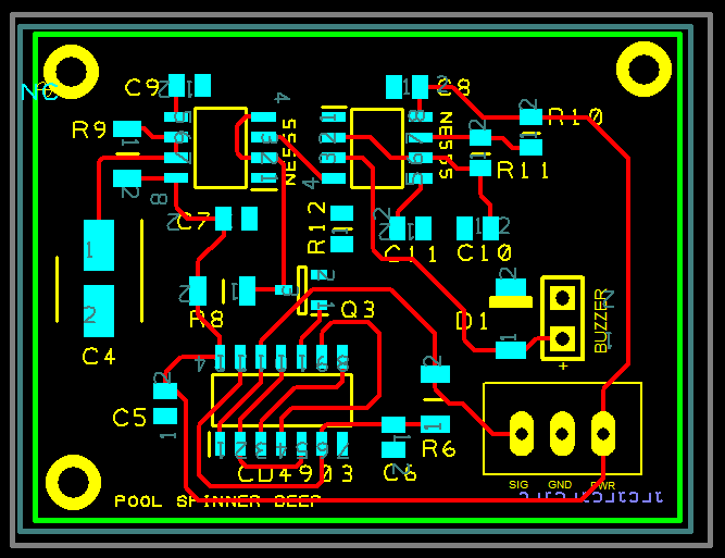
Made this using Design Spark.
2 layer board. All smd components. 2 connectors
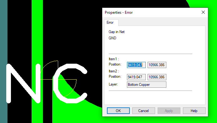
After i add the pours (top and Bottom) i run the rule checker i get this single error (Gap in Net (bottom Copper)
Perhaps I should not have a bottom copper pour? Could you fellas help me solve this?


2 layer board. All smd components. 2 connectors
After i add the pours (top and Bottom) i run the rule checker i get this single error (Gap in Net (bottom Copper)
Perhaps I should not have a bottom copper pour? Could you fellas help me solve this?
