Continue to Site

Welcome to our site!

Electro Tech is an online community (with over 170,000 members) who enjoy talking about and building electronic circuits, projects and gadgets. To participate you need to register. Registration is free. Click here to register now.

  • Welcome to our site! Electro Tech is an online community (with over 170,000 members) who enjoy talking about and building electronic circuits, projects and gadgets. To participate you need to register. Registration is free. Click here to register now.

Eagle Software Query

Status
Not open for further replies.
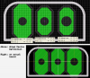
how to create in version 4.09r2? i've succeeded in creating the package , and the symbol but when i go to create the device and click on "add" i just cant find the symbol that i created in order to make the connections between the symbol and the package .

ps : when i go to look at the libraries i only find the package not the symbol besides him as all the components are
 
Hi fightstar,

the Eagle version you are running is really not of any importance. I'm running 3.5.5, 4.5.0 and 5.5.0 wich are almost the same with a few minor changes. (I also ran version 2.0.0 in the early 70s)

I prefer version 3.5.5 since it has less bugs than any other follow on version. Addionally it's colours are bright blue (solder side) and bright red (component side) compared with the pale colours used in succeeding versions. (not to be changed)

To create a symbol I guess there is nothing to tell about, but may be you missed an important detail: "SAVE".

Eagle goes strange ways sometimes. If you expect a symbol in alphabetic order it might appear miles behind the expected letter/number combination. (not experienced using version 3.5.5)

Just dig through your library and if the symbol is saved properly it will appear on the selection list sooner or later.

The problem is made by using ASCII code when putting (and sorting) names in the libraries, instead of logic sequence. (0 has a higher value than 1)

So, once again: dig through the library where you created the symbol. You'll find it 100%! :)

Regards

Boncuk
 
hi i ve done my eagle steps for my schematic and the board as well i ve got 100%, now i need to convert it to excellon and gerber formats in order to order an industrial panel with my schematic on it , how ?

thanks
 
I have not done it.

About all I know is that you need to run CAM job(s).

3v0

EDIT: It looks like the stuff at sparkfun is specific to their operation. But there is a tutorial on the SparkFun or BatchPCB site on the subject.
 
i knw now that the cam jobs on eagle are behind the conversions but i coudnt understand the steps to work with , could anyone help me on waht can i do to convert it ?
 
Hi fightstar,

an Exellon file is nothing but a CNC drill file.

It contains a list of tools (referring to drill bit sizes without actually stating the drill diameter) and the x-y coordinates of the drills in subdivisions pointing to the selected tool.

E.g. tool size 1 refers to a drill diamter of 0.4mm in your PCB-layout. Using a 0.6mm drill for tool no. 1 all holes in the sudivision of the list will be drilled with 0.6mm diameter.

From the control panel select CAM-jobs and select Exellon. Load the board and click perform job. The program will generate a file named <boardname.drd>.

This is what it will look like:

%
M48
M72
T01C0.0236
T02C0.0320
T03C0.0360
%
T01
X10195Y2156
X16320Y3687
X17695Y3094
X20195Y2156
X21851Y4437
X21163Y4937
X23663Y4906
X18288Y6344
X17351Y7844
X20695Y8937
X20195Y10187
X18195Y10187
X11507Y8531
T02
X2695Y1375
X3695Y1375
X4695Y1375
X5695Y1375
X6695Y1375
X7695Y1375
X8695Y1375
X9695Y1375
X10695Y1375
X11695Y1375
X12695Y1375
X13695Y1375
X14695Y1375
X15695Y1375
X16695Y1375
X17695Y1375
X18695Y1375
X19695Y1375
X20695Y1375
X21695Y1375
X21695Y11375
X20695Y11375
X19695Y11375
X18695Y11375
X17695Y11375
X16695Y11375
X15695Y11375
X14695Y11375
X13695Y11375
X12695Y11375
X11695Y11375
X10695Y11375
X9695Y11375
X8695Y11375
X7695Y11375
X6695Y11375
X5695Y11375
X4695Y11375
X3695Y11375
X2695Y11375
T03
X4320Y6375
X5320Y6375
X6320Y6375
X7320Y6375
X8320Y6375
X8320Y5375
X7320Y5375
X6320Y5375
X5320Y5375
X4320Y5375
M30

Not all of the information is necessary to drill a PCB. The PCB-manufacturer normally deletes certain lines of the file (lines two (M48) and three (M72) as well as the last line (M30)

Boncuk
 
Last edited:
Hi
since this thread appears to have a number of Eagle queries, does anyone have any idea why I am getting odd pad sizes ?
Basically, I have defined an e-line transistor device which has quite close pads (1.27mm apart). In the device definition, they appear correct, but when used on a board, it looks like the diameter is being ignored and always uses auto (I have done a library update). I am using 4.16

Have I missed something obvious ?

Mike
 

Attachments

  • eline_package.png
    eline_package.png
    29.1 KB · Views: 114
Status
Not open for further replies.

Latest threads

New Articles From Microcontroller Tips

Back
Top