Continue to Site

Welcome to our site!

Electro Tech is an online community (with over 170,000 members) who enjoy talking about and building electronic circuits, projects and gadgets. To participate you need to register. Registration is free. Click here to register now.

  • Welcome to our site! Electro Tech is an online community (with over 170,000 members) who enjoy talking about and building electronic circuits, projects and gadgets. To participate you need to register. Registration is free. Click here to register now.

EAGLE pcb software supposed to be easy?

Status
Not open for further replies.

MrDEB

Well-Known Member
I have looked at tutorials and still can't get a schematic started.
either I am stupid or ??
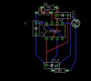
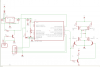
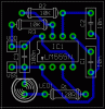
been using express pcb, very easy, user friendly BUT it does not output gerber files that I need.
For the project I am working on I plan on having about 6 boards made but them gerber files--grrr
ANY assistance in getting EAGLE or ?? going.
 
What are you stuck on?

Granted, EAGLE is not exactly instantly intuitive and has quite a learning curve, but you should be able to create a basic schematic/board after some basic fiddling...

I'd say one of the inhibiting factors in the beginning, is navigating the libraries and finding the parts you want. Getting used to that is half the battle...
 
Nobody ever claimed it was easy, that's for sure.

What tutorials have you tried? Try the Sparkfun one or follow along with one of the YouTube ones.
 
To add to what Mark suggests, the link below starts at lesson 1 from a series of about 12 tuts on youtube. I haven't looked at any of them, but they may be a start for someone new to EAGLE.


Regards.
 
Last edited by a moderator:
got lost using the sparkfun tutorial when it said to add 1XFRAME-LETTER:
where is this??
going to look at youtube tutorial, maybe help??
 
I first need sound.
When I put in a new HHD I nopw have no sound.
The device manager volume is disabled so thats out??
 
Mr.Deb, Just for you I created a Eagle tutorial. Keep in mind, I have only used Eagle for a short time so there are probably better ways of doing a schematic but this should get you started. Hope it helps. The file is a Word doc file.
 

Attachments

  • Eagle Cad Tutorial.doc
    323.5 KB · Views: 681
Let me know if it helps. Post your finished design :)
 
You should be writing instruction manuals. Your explanation worked GREAT.
Started laying out a pc board getting a feel for the commands.
I keep hearing about auto routing and optimization but haven't got that far yet.
will work on pc board design and then post
THANKS again
 
Here is how far I have gotten

Wish ? EAGLE had a wire bend feature like Express PCB
Kinda hard to put 45 miter s(Have yet to figure out the miter command in the menue display.
Can't move parts without ripping up then rerouting.
Now that I got past square one.
Need to add jumper points that connect PCboard to pannel mounted componets etc.
 

Attachments

  • led flasher.PNG
    led flasher.PNG
    17.2 KB · Views: 780
Wow, you already have a PCB, impressive :)
 
The tutorial was QUITE impressive! Hell I may start using EAGLE!

I use ExpressPCB too. I also found it easy to learn and use. I started using this so I could get experience in laying boards out so I could add the skill set to my resume. And got hooked on designing boards.

I have designed two simple PIC-centric boards in it and had ExpressPCB fab them. And they worked. The first had some really dumb mistakes, but number two was largely usable after assembly. My latest board is easily twice as large as previous boards, and uses copper filled planes in a double-layer board for easier power distribution. But that is proving trickier than originally thought. Perhaps I will post the final design here when I get done, but that will be days from now.

It's like building from an erector set: there are only a few types of pieces to build from, but the results can be really quite impressive if you apply yourself to the project. However, they don't autoroute (not necessarilly a bad thing), don't do bottom silkscreen, don't do internal slot routing, and when I found and reported that their DS1820 library part had Vcc and ground pins backward, they basically responded, "yeah, so?".

Just in case you didn't know, they will take your .PCB file and generate the Gerbers and Excellon drill files for $60. Then you are free to send them to cheaper fab houses for quantity fabrication. I have compared prices for the same boards I had ExpPCB build earlier, in the same small quantites, and there were no savings. The other places quoted 7 to 10 days turnaround and 1 to 3 day shipping, while ExpPCB offers 2 to 3 days to make them, then one ot two day delivery.
Have fun with your project.
kenjj
 
Last edited:
here is the schematic

need to add values. The component id is kinda convoluted .
for PC boardfs I am going to try this
DorkbotPDX | people doing strange things with electricity
If I get an order of say 6 boards pretty cheap
$5 per square inch you get 3 boards same design no set up fee
will work on tomorrow.
I found the bend tool
 

Attachments

  • CR combo eagle.PNG
    CR combo eagle.PNG
    29.7 KB · Views: 493
By Jove, I think hes got it. Good work. One comment though. You may find you have spacing issues when you start adding component values, but easy enough to fix :)
 
Last edited:
Nobody ever claimed it was easy, that's for sure.

Error!

Cadsoft claimed it to be easy. EAGLE stands for Easily Applicable Graphic Layout Editor.

Boncuk
 
Last edited:
Wish ? EAGLE had a wire bend feature like Express PCB
Kinda hard to put 45 miter s(Have yet to figure out the miter command in the menue display.
Can't move parts without ripping up then rerouting.
Now that I got past square one.
Need to add jumper points that connect PCboard to pannel mounted componets etc.

Hi MrDEB,

there is no reason why to make a simple PCB design double sided. Also the trace between pins 8 and 4 starts on the component layer and changes to bottom layer without via.

If the position of the LED is no issue you might use any location for it. There is still a lot of space to play with.

Also try routing traces at 45 and 90 degree bends. (The trace going off pin1 towards C2 has an acute angle.) Better use a 90 degree angle and manually draw wires on the junction to have two 45 degree angles.

Last not least never forget to draw a "frame" around the PCB design. Use layer20 (dimension) and trace width zero. Using the dimension "frame" you know exactly how to align the design on the copper clad for further process.

I also added two solder pads to connect to the power supply.

Boncuk
 

Attachments

  • 1ST-PCB.gif
    1ST-PCB.gif
    18.2 KB · Views: 1,126
  • T-JUNCTION.gif
    T-JUNCTION.gif
    6.1 KB · Views: 1,750
Thanks Boncuk. I was wondering when you are going to jump in.
I couldn't get EAGLE started up. Mikebits posted a simple tutorial that jump started the learning process. Will look for and try the layer20 and what is trace zero?
The led flasher board is my very FIRST try using EAGLE (EASY, yea right!) they need better tutorials like Mikebits posted.
I need to get on the fast track so I can start putting this creature to market.
Contemplated going all surface mount but have NO real experience using. Present design uses SMD on all the resistors. Need to start somewhere.
At $5 per square inch but you get 3 of same design so it works out to $1.60 per square inch. At least thats what I come up with.
DorkbotPDX | people doing strange things with electricity
 
Status
Not open for further replies.

New Articles From Microcontroller Tips

Back
Top