Electro Tech is an online community (with over 170,000 members) who enjoy talking about and building electronic circuits, projects and gadgets. To participate you need to register. Registration is free. Click here to register now.
Welcome to our site! Electro Tech is an online community (with over 170,000 members) who enjoy talking about and building electronic circuits, projects and gadgets. To participate you need to register. Registration is free. Click here to register now.
Hi,
For the track overlapping the pad, it is not the problem. The pad gets the higher priority when it's printed out. As for the pad for the transistor, you can add a bigger pad on it. It is in wirepad library.
Hi,
For the track overlapping the pad, it is not the problem. The pad gets the higher priority when it's printed out. As for the pad for the transistor, you can add a bigger pad on it. It is in wirepad library.
Hmm.. the overlapping means they are connected. Those not overlapped are not connected actually. If you want them to be not overlapped and connected visually, just remove the wire and reconnect it without touching the hole of the pad.
But there is! Use Eagle 5 and proceed as if you were going to print the artwork. In the print dialog box click on PDF, it will create a PDF file of your artwork. A few hours ago I posted a note about using PDF for schematics. Never try to make a PCB using EXPORT>IMGAGE.
If you want larger pads in general increase the size of restring in the DRC.
Also the pads and traces will not generate the overlap error if they have the same name. Check the name of the pad and all traces that connect to it. Change them if needed so they all have the same name.
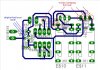
The layout is done direct placing the components (not via the schematic) that why it took me 4 hours to draw this
But there is! Use Eagle 5 and proceed as if you were going to print the artwork. In the print dialog box click on PDF, it will create a PDF file of your artwork.
Oooooooops I'm using Eagle professional edition.Mmmm I like to buy the Eagle 5 (don't know free version allow to do this).Thats really nice If I can export directly to the PDF format.
3v0 said:
Also the pads and traces will not generate the overlap error if they have the same name. Check the name of the pad and all traces that connect to it. Change them if needed so they all have the same name.
Oooooooops I'm using Eagle professional edition.Mmmm I like to buy the Eagle 5 (don't know free version allow to do this).Thats really nice If I can export directly to the PDF format.
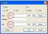
I guess you made the routing using a grid size of 1/40". To avoid overlapping errors switch to grid size 1/80" and move the trace connecting the relay to the left by one click. For a 45 deg reference line use either the dimension (20) or the tPlace (21) layer and a trace width of zero.
By moving the trace one click (1/80" (0.3175mm)) the overlap error should be eliminated. For the 45 deg bend use the suggested method or you'll probably trade an overlap error for an angle error.
Pads too small? No problem. Copy and paste the package. Change the pad size and if necessary the drill size and save the package. Create a new device using that package. Erase the old one from the board and use the new one.
If the PCB is created on the base of a schematic it can be replaced without loosing too many of the traces. I have replaced 40pin MCUs without any problem. Just mark the position of the device (package) on the PCB using the above described method, this time marking an X. Place the new and connected device exactly on the position of the old one and use rats nest.
The resulting picture should not leave more than 5mm of trace to route new for each pin, and all air wires going straight into the pin they should connect to.
Also the pads and traces will not generate the overlap error if they have the same name. Check the name of the pad and all traces that connect to it. Change them if needed so they all have the same name.
I guess you made the routing using a grid size of 1/40". To avoid overlapping errors switch to grid size 1/80" and move the trace connecting the relay to the left by one click. For a 45 deg reference line use either the dimension (20) or the tPlace (21) layer and a trace width of zero.
Just open and played with your board. What you are trying to do is a lot like buying an airplane and trying to drive it on the road.
Best
Draw a schematic, when you create the board it will provide air wires for all required traces. Then all you have to do is place the parts and convert the air wires to traces by routing them with the route tool. You then have a board that matches the schematic.
Not So Good
Skip the schematic. Place the parts on the board then connect the pads using the signal tool, this creates air wires. Convert air wires to traces using the route tool. [
BAD (what you are doing)
Skip the schematic. Place the parts on the board. Use the wire tool to draw traces as need. It will make a new signal (name) every time you draw a new trace. Since the pads already have names the traces you connect to them will not be the same name as the pad. That is the source of most of your overlaps.
Air wires are not unique to Eagle. Most good layout packages use them, even without schematic capture. The idea is if you tell the program what you want to connect (draw signal), it will help you place the trace (route it).
I hope this makes sense. If not let me know and I will try again. Once you get the hang of the schematic editor you will not ever want to do a board without first making a schematic.
adjusting the grid size is sometimes a bit annoying. Move the cursor into the field you want to change. Press the "Home" key and delete the content using the "Del" key. Then replace with new values. (Overwriting will most probably cause problems.)
Don't use a comma instead of a dot. You'll receive an error message and Eagle continues with the original values. (No change effective.)
I loaded Guyan's file. It is not a grid problem. He is getting the overlap errors because the names on the traces do not match the pads they connect to. This is because he created the traces with the wire tool.
Fix the problem by removing old traces, adding the air wires between pads. and route the traces between the pads using the route tool.
I fully agree. It is the greatest nonsense not to use air wires, even omitting a schematic.
Just let me put it this way: He is using Eagle as a "paint program" and wonders why it produces nonsense.
Hi Gayan,
just follow these rules when working with Eagle. Make a neat schematic first and check for connection errors. It is a good idea to activate the pin layer to check if the connected pins highlight when clicking with the eye-symbol. Also have the ERC check done before you type "board;". The resulting PCB is error free with all parts connected properly as air wires.
Use the routing tool to connect the parts properly. A grid size of 0.25inches will do for rough routing. If space becomes a problem change to grid size 0.125inches and move the traces by just one click.
Also try to keep traces as straight as possible. Junctions and intersections should be enforced. (Check the highlighted trace on the sample picture.)Electrically this is a good way and optically it just looks better. Electronic devices should not only work. They should also look beautiful from the design.
I didn't download your zip file, but made the same circuit just using air wires. There was absolutely no DRC error in this PCB design. Just for safety reasons (soldering without solder mask) I rerouted some bends into the traces underneath the resistors.
The resulting PCB layout looks neat and additionally you don't get into trouble when soldering.
BTW, your circuit won't work at all! There is a very important detail missing. Pin4 (supposedly ground pin of the IC) is not connected!
Hi thanks for both of you.Last night I did a through search in eagle.
What I did was placed the components & make air wires using the signal tool.After I took the Route tool & route the traces.But when I see the layout or when I export the file the traces it still overlaps the pad.The name of course same in this case.I don't know how to solve this.
Why do I need to export?
Because I need to export the layout image, I'm not directly printing from eagles print.Just to show the PCB layout for someone else I need this image saved to some other format.
Boncuks method!
I tried changing the Grid size the problem solved mostly.Making a higher resolution Grid size makes smoother movements in the components & traces.Ex: (1/100)
But I need to solve this overlap thing using 3V0 s method.(Make signal & using the route).
Because I need to export the layout image, I'm not directly printing from eagles print.Just to show the PCB layout for someone else I need this image saved to some other format.
This site uses cookies to help personalise content, tailor your experience and to keep you logged in if you register.
By continuing to use this site, you are consenting to our use of cookies.

")