Electro Tech is an online community (with over 170,000 members) who enjoy talking about and building electronic circuits, projects and gadgets. To participate you need to register. Registration is free. Click here to register now.
Welcome to our site! Electro Tech is an online community (with over 170,000 members) who enjoy talking about and building electronic circuits, projects and gadgets. To participate you need to register. Registration is free. Click here to register now.
Have you looked in: ic-package.lbr ? Which version of Eagle are you using? If you still can't find it, go cadsoft.de , click on downloads, then libraries and download what you need. John
If it's also the circuit symbols you need, you'll have to **broken link removed** to create a custom part. Even if you do find ic-package.lbr on your system or on the web, I still recommend trying the tutorial at least once because you'll be able to make up your own custom stuff for any situation.
To summarize the whole tutorial, you'll need to open EAGLE's control panel window and go to: File > New > Library.
1. Find and click the symbol icon on the window that appears.
2. Make up a name for the symbol (example: ADC0808) in the window that appears. Click OK. Then YES, if asked.
3. Draw out the part using lines, circles, rectangles, etc...
4. Place pin locations using the pin icon (below the drawing icons on the sidebar)
5. Place text for >NAME, >VALUE (make sure to change their layers to "name" and "value" also). Save progress.
6. Click the package icon at the top
7. Choose a name for the package (example: DIL28)
8. Draw the footprint you want (>NAME, >VALUE)
9. Place and edit pins (make sure number of pins matches your previous drawing). Save progress.
10. Click the Device icon at the top
11. Select the device name you came up with in step 2.
12. Click the add icon on the sidebar
13. Drop your symbol onto the workspace.
14. Click the NEW button in the bottom right.
15. Select the package name you came up with in step 7. Click OK.
16. Click the Connect button (next to the "NEW" button from step 13)
17. In the window that appears, match the symbol's pins to your package's pins with the long "connect" button. Click okay when done.
18. You're done. Save everything and now you can use that custom part in any project.
...Maybe my list is missing some minor stuff, so I really recommend doing it by the tutorial. If time is critical or a custom part just seems like overkill, just download the ic-package.lbr file from EAGLE.
I observe that many people seem to have problems with Eagle. I have about 25 years of experience with Eagle starting at the first DOS-version.
I also made a translation of the manual including lots of illustrations and examples how to use Eagle without getting headaches.
Especially when creating new parts (not available at CadSoft) there are very easy ways to go and finish a part in almost no time. Try to find a chip named TC7SH08F. No luck! It's a single HC-AND-gate in an SOT-23-5 package. Once you have made the package the rest is a piece of cake.
If you think it will be a good idea to use the translation as a kind of help file just give me hint how to post it here for everybody interested in it.
I mean, not like a normal post asking a question, but as a constant reference which I will update from time to time. However I don't know how to do that.
In a poll in August, 2005, 15 of 17 respondents used Eagle for schematic drawing and capture. See: **broken link removed**
Questions regarding Eagle are frequent enough that I think a separate sub-forum, perhaps in Electronics Content, would be better than a sticky. The forum could have its own stickies. The problem I foresee with just having a sticky for Eagle in another forum is that it might get quite lengthy and rarely read. John
Edit: I don't mean that the sub-forum would be called Eagle. Something generic, such as Schematic Design, etc. would probably be more appropriate.
I observe that many people seem to have problems with Eagle. I have about 25 years of experience with Eagle starting at the first DOS-version.
...........
On your schematic, just add a jumper(s) (solpad library), and name the net. Place on board. It doesn't matter what layer the jumpers are, they are symmetrical.
You can also just add a via directly to the board, properly name it (e.g., gnd), and it will be connected to ground in the pour. It will not have thermals, though. It is far better, in my opinion however, to do it on the schematic.
I am not aware of a stand-alone app to do what you want with the libraries. Version 5.xx is supposed to have library management enhancements. I just bought my copy, but won't have the activation code until Wednesday.
sorry but my question was asked hastly and forget to ask how let EAGLE to create "jumpers" with the autorouter, I mean let eagle create the most of the wires in the bottom layer and create few only wires (let say jumpers in this case) in the top layer. because, almost of us have some difficulties to configure the autorouter settings .
If you are asking whether you can force Eagle to use only one layer, yes.
So far as I know, Eagle does not create jumpers in the autorouting process. Jumpers are "devices" and must be added to the schematic as I already described. Eagle will show unrouted connections (nets) after autorouting, but it is up to you to add jumpers, if necessary.
I would not depend on the autorouter and rarely use it only to get ideas for placement and where problems may be. Then I rip-up completely and route manually.
there is always the possibility of misinterpretation of the term "jumper". From my point of view a jumper is a device with two or three pins and therefore must be contained in the schematic. E.g. it gives the choice to either ground an input or tie it to VCC.
The term "jumper" is clearly defined in the German language as "Steckbrücke", whereas a "jump" (as I call it) is defined as "Drahtbrücke". (to connect two car batteries you don't use a "jumper cable", but a "jump cable". )
Jumps are made to connect two points of an interrupted trace using a piece of wire.
Even using the autorouter jumps can easily be made having most of the circuit routed on the copper side only, leaving some air wires, just because Eagle tends to surround itself. Check the routing thoroughly and I bet you'll get one or another laugh about the stupid routing. Correct routing as far as possible.
Go through the autorouting process again, this time activating the component layer for routing, leaving the solder side unchanged.
When routing is complete check if you can apply changes to straighten the traces on the component side.
Mark and label the jumps on the component side using thin lines (1/200") between two vias. Ripping up the connection between two vias will probably result in erased vias.
Planning for your selfmade board just don't print the component side and use the traces on the component side as a reference when placing parts (not to forget any jump).
Sending the PCB layout to a PCB manufacturer you must insist on a single layer board and ignore the component side traces.
To make sure you won't get an expensive double layered board you might rip the traces on the component side and replace the "lost" vias manually. Name both sides of the (interrupted) net equally and there will be a (hopefully straight) air wire between those vias after using rats nest.
This board layout might be turned in for manufacturing wihtout resulting in a double layer PCB.
There is always enough space to keep the jumps straight.
and if some one here in this forum control well the autorouter and his setting, how to use them ,tricks or some tutorial, web links..... please let me know.
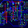
Can you please tell me how you did these forms when routing the wire i.e triangular or polygones wires (of course with the autorouter not manualy!!), look to the image joined.
Can you please tell me how you did these forms when routing the wire i.e triangular or polygones wires (of course with the autorouter not manualy!!), look to the image joined.
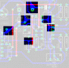
you can't use the autorouter to do that. It routes straight (if at all). Junctions of traces can be made like this:
Draw a normal straight trace routing manually or even using the autorouter. When routing is finished look use a wire of the same layer and thickness as the trace. Switch routing direction to 45degrees and set two pieces of wires as shown in the picture. The "enforcements" should slightly overlap the original trace for a solid area.
This site uses cookies to help personalise content, tailor your experience and to keep you logged in if you register.
By continuing to use this site, you are consenting to our use of cookies.

") with you all.
with you all.