Electro Tech is an online community (with over 170,000 members) who enjoy talking about and building electronic circuits, projects and gadgets. To participate you need to register. Registration is free. Click here to register now.
Welcome to our site! Electro Tech is an online community (with over 170,000 members) who enjoy talking about and building electronic circuits, projects and gadgets. To participate you need to register. Registration is free. Click here to register now.
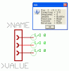
connectors normally have pin and pad names being the same. IC's might have different pin and pad names, e.g. pin name "\MCLR", pad name "1".
When designing the symbol use "Change - Visible - pad" and give the pin a name. Design the package assigning a name for each pad.
Finally use both - symbol and package to create a device. Connect pin1 and pad1, pin2 and pad2, etc.
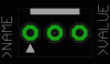
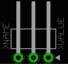
Using the new device in a schematic pins are displayed with pad numbers. Switching to "board" the device has no visible pad numbers (as per package design), but a pin1 arrow. When drawing the arrow make sure to have it outside the tStop-layer (29).
Any drawing made within tPlace-layer (21) will be printed on the final design (component print). Arrows printed inside tStop-layer will be printed on solder pads which is not desirable for good soldering work.
This site uses cookies to help personalise content, tailor your experience and to keep you logged in if you register.
By continuing to use this site, you are consenting to our use of cookies.