Continue to Site

Welcome to our site!

Electro Tech is an online community (with over 170,000 members) who enjoy talking about and building electronic circuits, projects and gadgets. To participate you need to register. Registration is free. Click here to register now.

  • Welcome to our site! Electro Tech is an online community (with over 170,000 members) who enjoy talking about and building electronic circuits, projects and gadgets. To participate you need to register. Registration is free. Click here to register now.

eagle help please

Status
Not open for further replies.

dasatboy

New Member
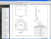
Guys I am trying to use an ATtiny2313 MLF package in my project.

I could not find the proper device alread done. So I tred to add my own. Following the guide on eagles site. i created the part in schemtic editor adding the pins. and naming them.

Then I created the package.

Then I matched the pins to the pads when creating a device.


When I add my new device to the drawing and run lines to the other components, the airwave lines don't show up! And when I choose "Show" and click the pad I want to connect to the new device the appropriate pad does not chow up.

Anyone got a better guide? Or any ideas. Attached is a copy of the library.

ThankS
 

Attachments

  • lib.zip
    8.4 KB · Views: 126
I added your library and made a trial schematic with the same result you got. I did notice the attachment point of your pins was odd, so I went back to the symbol and noticed they were attached backwards. The little open circle (attachment point) should be away from the outline, not on the outline.

I then went back and did another trial schematic intentionally making my airwires attach to the base of the pins, and everything worked as expected.

So, the problem seems to be that the pins were attached to the symbol backwards. You can unassemble the device, edit the symbol, etc. to fix it, or just try to use it as is, but make your attachments to the base of the pin, not the end as usual.

BTW, ERC did not like the attachment and gave lots of overlap warnings. So, I would recommend the first option of trying to fix the symbol rather than doing a work around. Also, when you save something be sure it is done with "show all" selected before saving.

John
 
Nice catch it worked flawlesly! Now being a complete rookie and such I have been working with Through hole deign. and some SMD.

This device I am trying to make a library of, I am going off the data sheet from ATMEL. As seen in the below attachment.

I had assumed that the the 4BSC measurement was 4mm. Thats really small! I am second guessing it! Can anyone shed some light on this?
 

Attachments

  • scpinout.JPG
    scpinout.JPG
    167.3 KB · Views: 161
I had assumed that the the 4BSC measurement was 4mm. Thats really small! I am second guessing it! Can anyone shed some light on this?

If you divide the 4mm by 10 you're pretty close to the real dimension. :D
 
Are you telling me the size of this chip is .04mm x .04mm. thats even smaller? not sure about this! LOL I should just add one to my digikey order next week ans see.
 
If you divide the 4mm by 10 you're pretty close to the real dimension. :D
Come on Hans, you are joking, right? :)

I had assumed that the the 4BSC measurement was 4mm. Thats really small! I am second guessing it! Can anyone shed some light on this?

Could that be because right below where is says 'Common Dimensions' it says unit of measure = mm.?

If D2 and E2 are 2.60 mm (nominal)
then the chip must measure 4.0 x 4.0 mm.

0.5 mm between contact centers seems correct.
 
Are you telling me the size of this chip is .04mm x .04mm. thats even smaller? not sure about this! LOL I should just add one to my digikey order next week ans see.

I'm telling you the pin spacing. Body size is of minor importance and is almost automatically done with the proper pin spacing.
 
Thanks guys! Never really thought the over all size was important. Just haddn't seen these chips in that form. Seemed kind of small. I am still going to order one and etch a test board. See how dificult it will be for the average home user to install these. (I do have a HAS)!

Thanks for all the help!!!

Hi dasatboy,

the overall size will become important if the part jumps off your PCB while soldering and drops to the floor.

Here is a hint for successful searching: Use a vacuum cleaner and "scan" the entire room.

If you hear a faint click you'll know you have found the part. :D

Small SMD-parts almost have the same behaviour as the needles of the christmas tree. The last ones are found around Easter. :)
 
Status
Not open for further replies.

New Articles From Microcontroller Tips

Back
Top