Continue to Site

Welcome to our site!

Electro Tech is an online community (with over 170,000 members) who enjoy talking about and building electronic circuits, projects and gadgets. To participate you need to register. Registration is free. Click here to register now.

  • Welcome to our site! Electro Tech is an online community (with over 170,000 members) who enjoy talking about and building electronic circuits, projects and gadgets. To participate you need to register. Registration is free. Click here to register now.

Eagle cad routing help

Status
Not open for further replies.

aruna1

Member
hi guys
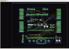
I'm making a PIC development board and need your help.
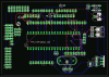
i made the schematic,and kind a stuck with routing it.auto router isnt doing goodjob of routing it.
can some one give me a hand here? (this is the first time i'm using eagle cad)
i have attached relevent files here.

full file set
**broken link removed**
 

Attachments

  • pic board..zip
    786.7 KB · Views: 194
Auto router will give you the nearest possible as much it can.The other balance you must do by using the router tool.

When I'm doing a PCB I won't auto route.I draw the schematic & click the board icon so you get the ratnest.After I place components to the best place where it minimizes jumpers & overlapping lines.Finally I'm routing manually by the use of route tool.
 
Last edited:
Hi aruna1,

you're making your life tough using a grid size of 3mm for the PCB layout.

Most parts are manufactured using imperial measurement. Using a metric scale routing becomes extremely difficult and ends in a never stopping "angle" and "overlap" error list when performing a DRC.

I suggest to delete the PCB and create a new one. Use a grid size of inches and a fraction thereof. If you're used to metric scaling use the windows calculator to define the grid size in mm instead of inches.

1 inch equals 25.4mm, 1/2 inch=12.7mm, 1/4 inch=6.35mm etc. Using the equivalent metric value traces will be straight from pin to pin. Otherwise the router has to jump to "snap" and makes funny bends.

Ratsnesting your designed PCB there are lots of crossing airwires, meaning routing will become almost impossible unless you use multilayer.

If you must do that because of a prescribed position of connectors you should really think about a multilayer board design.

Boncuk

P.S. No wonder the file size of the zip file was very large. You also zipped the backup files!
hi i didn't get what you said,can you explain little bit more
 
Auto router will give you the nearest possible as much it can.The other balance you must do by using the router tool.

When I'm doing a PCB I won't auto route.I draw the schematic & click the board icon so you get the ratnest.After I place components to the best place where it minimizes jumpers & overlapping lines.Finally I'm routing manually by the use of route tool.

A point to add here, since one cant know the optimum position for setting up the component positions what i do is make several copies of the same board. I try one thing and try to work it out, if it doesnt then move on to another, hard work but the final product is worth it. Also if you want it easy then i have heard that there is this software called circuit designer which places the components for you and also routes them( dont know how good it is though). But i will second what every body else has said that auto routing sucks. period.
 
A point to add here, since one cant know the optimum position for setting up the component positions what i do is make several copies of the same board. I try one thing and try to work it out, if it doesnt then move on to another, hard work but the final product is worth it. Also if you want it easy then i have heard that there is this software called circuit designer which places the components for you and also routes them( dont know how good it is though). But i will second what every body else has said that auto routing sucks. period.
For the type of Development board, it is imperative to have all connectors oriented in the same angle.The main goal appears to bring out all ports etc.
the component positioning may not be possible. the auto layout may have to be accepted with minor changes done judiciously. I tried with Red and Blue layers to have any routing by using"*" option.
Perhaps Aruna1 may have to accept it.
 
Last edited:
For the type of Development board, it is imperative to have all connectors oriented in the same angle.The main goal appears to bring out all ports etc.
the component positioning may not be possible. the auto layout may have to be accepted with minor changes done judiciously. I tried with Red and Blue layers to have any routing by using"*" option.
Perhaps Aruna1 may have to accept it.

Hi Sarma, you are right. I forgot to mention that excluding the ports, of course you first set the ports on the outer boundaries of your board on the sides that you want.But when you have certain IC's like say a microcontroller, you can flip it upside down for ease . This is what i had to do in my PICDEMZ clone. The auto router in Eagle is sort of primitive, or may be auto routing itself is just in its primitive phases.
 
Hi arun1,

here is a screenshot of your original PCB layout.

Notice the grid size in the upper left hand corner.

It says clearly "3mm". With that grid size you don't do yourself any favour.

Delete the board and create a new one.

That's the best advise I can give you. Also place the connectors close to the MCU-pins for easy routing.

Rearranging MCU pin connections and connectors the PCB can be made single sided.

The screenshot shows you the rough board design with the pins connected as per your schematic.

One word referring to schematics: It's no good practice to draw nets through the outline of an IC. Pin names become unreadable and the overall picture makes a bad impression.

If you don't have enough space to design on A4-format use A3. When printing use scale factor 0.7 for a format filling A4 paper sheet.

Boncuk
 

Attachments

  • PIC-BOARD..gif
    PIC-BOARD..gif
    59 KB · Views: 340
  • PIC-BOARD-01..gif
    PIC-BOARD-01..gif
    40 KB · Views: 382
A point to add here, since one cant know the optimum position for setting up the component positions what i do is make several copies of the same board. I try one thing and try to work it out, if it doesnt then move on to another, hard work but the final product is worth it. Also if you want it easy then i have heard that there is this software called circuit designer which places the components for you and also routes them( dont know how good it is though). But i will second what every body else has said that auto routing sucks. period.

I sure disagree with your auto router thinking and if you know what you're doing Eagle has a very robust auto router and is capable of extremely nice boards. Your DRC file controls the behavior of the router and how you lay out the components. Here is a very complex board done by Eagle with a continuous reverse ground plane on a 5 mill grid. 100% routed as well.

**broken link removed**
 
@Boncuk, Nice workout !!

t looks much simpler in its new component overlay.

Hi mvs,

thanks for the flowers. :)

If the OP decides to connect MCU and connector pins in an altered (and logical) sequence he can shrink the PCB a bit more. That "design" took me 20 minutes with the board size shrunk 20mm in height.

Did you also take a look at the schematic, and would you like to read it for trouble shooting?

Regards

Boncuk
 
Status
Not open for further replies.

Latest threads

Back
Top