Continue to Site

Welcome to our site!

Electro Tech is an online community (with over 170,000 members) who enjoy talking about and building electronic circuits, projects and gadgets. To participate you need to register. Registration is free. Click here to register now.

  • Welcome to our site! Electro Tech is an online community (with over 170,000 members) who enjoy talking about and building electronic circuits, projects and gadgets. To participate you need to register. Registration is free. Click here to register now.

Driving PMOS with Darlington Transistor Array

Status
Not open for further replies.

EvilGenius

Member
Hello
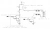
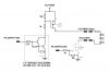
I designed the attached circuit and when I built it, it behaves oddly.
The circuit is to drive a 12V, 3A LED Module (for simplicity). The inputs are from 2 pins of microcontroller (PIC @5V).
One pin controls one channel of NPN darlington transistor array (Darl-NPN) connected to gate of a PMOS to provide 12V Drive output voltage and current to LED module. The second pin drives an NMOS to sink the current to ground from LED module. The specifics of each component is provided.

Issue: It seems like the PMOS is staying on at all times although the bias and pull-up should have turned it off when no voltage (current) is coming from PIC Pin1. My guess is that the darlington array with hfe of 1000 is so powerful in amplification that smallest voltage (leakage) turns it on and keeps it on.

Any help or suggestions is very much appreciated.
Regards, Rom
 

Attachments

  • 1.jpg
    1.jpg
    132 KB · Views: 976
Look again at the P-MOSFET drain and source connections. You have the source and drain interchanged, thus the current is being continuously carried through the forward-biased substrate parasitic diode. (The substrate arrow on the MOSFET symbol shows the direction of the diode current flow. You normally want that diode reverse biased).
 
Look again at the P-MOSFET drain and source connections. You have the source and drain interchanged, thus the current is being continuously carried through the forward-biased substrate parasitic diode. (The substrate arrow on the MOSFET symbol shows the direction of the diode current flow. You normally want that diode reverse biased).
Crap. You are right. PMOS is reverse of NMOS. Current goes from Source to Drain. (Emitter to Collector). Thanks!

Now I have to reconfigure the entire PCB or do a heart bypass!
 
Last edited:
Sorry, but current (not electron flow) is from source to drain in a P-MOSFET. Both NMOS and PMOS symbols have the drain on the top and the source on the bottom.
Why did you think it was the reverse?
 
Sorry, but current (not electron flow) is from source to drain in a P-MOSFET. Both NMOS and PMOS symbols have the drain on the top and the source on the bottom.
Why did you think it was the reverse?

According to datasheet PMOS has Source on Top while NMOS has the Drain on top (reverse biased internal diade as you said). You had it correctly the first time. In PMOS current flows from Source to Drain. While in NMOS the current flows from Drain to Source. I am looking at datasheet for FQP17P06 vs. FQPF13N06L. Please confirm my findings. It would have been easier for them to stick to Base, Emitter, Collector as it would make more sense to me. in PNP current goes from Emitter to Collector. In NPN the current goes from Collector to Emitter.

Regards,
Rom
 
According to datasheet PMOS has Source on Top while NMOS has the Drain on top (reverse biased internal diade as you said). You had it correctly the first time. In PMOS current flows from Source to Drain. While in NMOS the current flows from Drain to Source. I am looking at datasheet for FQP17P06 vs. FQPF13N06L. Please confirm my findings. It would have been easier for them to stick to Base, Emitter, Collector as it would make more sense to me. in PNP current goes from Emitter to Collector. In NPN the current goes from Collector to Emitter.
The problem is, that data sheet showed the P-MOSFET symbol with the source on the top, which is not the usual orientation, but normally the source is always more positive than the drain in either case.
I don't understand your confusion about this and why you think the symbols for BJTs are more clear. :confused:
So in the schematics above in the post both PMOS and NMOS are in the wrong directions?
 
I looked at several examples and usage of NMOS and PMOS. Thank you for pointing out the issue.
In all examples PMOS is used as Source on top with higher voltage. While in NMOS Drain is on top at a higher voltage.
Another words: Source=Emitter, Drain= Collector. In PNP (PMOS) current enters the device from Emitter (Source). In NPN (NMOS) current enters from Collector (Drain) for forward bias.

You are overlooking a very important point. That is how the gate is driven in a PFET vs how it is driven in an NFET.

To turn on an enhancement-mode NFET, the drain is positive, the source is negative, and the gate must be more positive than the source by Vt plus a couple of Volts.

To turn on an enhancement-mode PFET, the drain is negative, the source is positive, and the gate must be more negative than the source by Vt (negative number) minus a couple of Volts.

Thanks MikeML. I am not overlooking those points they are already in the design. As you can see in the shcematics this was taken into consideration. Also pullup and pulldown resistors were added to help in fast switch-off and to prevent false trigger.
 
Thank you gents for your responses. I already made the correction in the design and will burn a new board. Cheers.

Updated Schematics below:
 

Attachments

  • 1.jpg
    1.jpg
    126.3 KB · Views: 252
Last edited:
So in the schematics above in the post both PMOS and NMOS are in the wrong directions?
No, only Q3 is in the reverse direction. Q4, the N-MOSFET, has current going from drain to source as is normal.
 
Hey Evil,

begs the question. Why do you even need the PFET? Just tie the top end of the LEDs to +12V, and let the NFET do the switching. Saves a port pin on the PIC, too.
 
Hey Evil,

begs the question. Why do you even need the PFET? Just tie the top end of the LEDs to +12V, and let the NFET do the switching. Saves a port pin on the PIC, too.
Mike
This is one circuit of 12 channels. It is 12 channels multiplexed RGB. 15 pins of PIC control the multiplexing: 12 pins drive 12 channels of darlington array, driving PMOS's.
3 pins drive the NMOS (sinks). (12 Mux 3)
I need the MOSFETS for high current driving of 12V, 36A (3A per channel).
 
Schematics has been Modified once again. 3K ohm resistor has been removed. Circuit has successfully tested.
 

Attachments

  • Darlington Array PMOS Driver.pdf
    20.2 KB · Views: 367
Status
Not open for further replies.

New Articles From Microcontroller Tips

Back
Top