Hi,
I am driving an irf640 mosfet with ir4427. Vg is 12V . for the mosfet Qg is 83nC. from Microchips documentation Ig = Qg/T(trans)
the driving pulse is 50Khz. so T(Trans) = 1/50000. From the above equation I calculated Ig to be .00415 Amps.
The gate resistor value would be 2891.5 Ohm.
Am I correct in my above calculations.
VDD is 100V and Id = 11Amps........
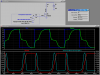
The problem is that the mosfets get very very hot just after 1 min and I have to switch off!. Currently I do not have the luxury of a scope as it is out on loan!!!!..
Any help is appreciated
cheers .. Emmkay.
I am driving an irf640 mosfet with ir4427. Vg is 12V . for the mosfet Qg is 83nC. from Microchips documentation Ig = Qg/T(trans)
the driving pulse is 50Khz. so T(Trans) = 1/50000. From the above equation I calculated Ig to be .00415 Amps.
The gate resistor value would be 2891.5 Ohm.
Am I correct in my above calculations.
VDD is 100V and Id = 11Amps........
The problem is that the mosfets get very very hot just after 1 min and I have to switch off!. Currently I do not have the luxury of a scope as it is out on loan!!!!..
Any help is appreciated
cheers .. Emmkay.
")
