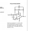
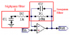
Hello, I've been checkin' some distortions for electric guitars and have seen that some of them use common collectors in the first and last stages because of their input and output impedances. But there's something I don't understand, in this site I saw that they add a low pass filter and a high pass filter, but they put it in the feedback path, and is a way that I don't understand, as I know, a passive low pass filter is a resistance in series with a capacitor and you take the output from the capacitor, and for vice versa for the high pass filter. I don't know if that's some kind of band pass filter, but in the explanation they say that the low pass filter is made by C1 and R1, and the high pass filter by R2 and C2. But why are they in the feedback path? why are R2 and C2 in the high pass filter in parallel? from where do you take the output? and from where do you take the output in the low pass filter?
Thanks in advance.
Thanks in advance.