Continue to Site

Welcome to our site!

Electro Tech is an online community (with over 170,000 members) who enjoy talking about and building electronic circuits, projects and gadgets. To participate you need to register. Registration is free. Click here to register now.

  • Welcome to our site! Electro Tech is an online community (with over 170,000 members) who enjoy talking about and building electronic circuits, projects and gadgets. To participate you need to register. Registration is free. Click here to register now.

differential pair-single ended to differential signal converter

Status
Not open for further replies.

penny07

New Member
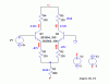
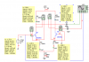
Hello,currently i'm designing single ended to differential signal converter.I use differential pair with emitter resistor.In order to get the Q-point,i have to know about my Vce cutoff point.But, the problem is i'm not sure what is my Vce cutoff point.Below is my attachment about my circuit~
Thanks~
 

Attachments

  • design.PNG
    design.PNG
    33.3 KB · Views: 332
hi penny,
How did you get those values in the yellow text boxes.??

With a 8Vppk sine wave input the collector signals are grossly distorted and those values are meaningless.

Try a 1Vppk signal , also consider a constant current source for emitter drive

E
 
i use measurement probe to get those yellow boxes.How to know that the maximum of the input signal can be applied to avoid the distortion to occur?because the assignment requests us to find out the reason behind~and what do you mean a constant current source emitter drive?
thanks:)
 
i use measurement probe to get those yellow boxes.How to know that the maximum of the input signal can be applied to avoid the distortion to occur?because the assignment requests us to find out the reason behind~and what do you mean a constant current source emitter drive?
thanks:)

hi,
Tell me what you calculate the gain of the amplifier to be.?

Once you know that you can determine what the maximum input can be before the amplifier distorts the signal.

The current source would be in the emitter/s circuit of the amplifier.

Google for 'transistor differential amplifier'

https://www.st-andrews.ac.uk/~www_pa/Scots_Guide/audio/part1/page3.html
 

Attachments

  • files_3-Handouts_Handout_5b.pdf
    783 KB · Views: 592
Last edited:
my gain is 0.5 and actually 900ohm and -5V is my design of current source~and got any equations can be used to calculate and prove that when it reaches the maximum input,the output signal will start to distort?because when i do my simulation, i found out that when my input is 2.7Vppk, the output signal start to be cutoff.
Thanks:)

circuit.png
simulation.png
 
Last edited:
my gain is 0.5 and actually 900ohm and -5V is my design of current source~and got any equations can be used to calculate and prove that when it reaches the maximum input,the output signal will start to distort?
Thanks:)

hi penny,
All the equations you need are explained on the pdf I posted.

Look at this image.

E
 

Attachments

  • AAesp01.gif
    AAesp01.gif
    30.6 KB · Views: 287
hi penny,

This simulation of your circuit was done using LTSpice.

I have used a ramp input signal, you should be able to confirm your distort level input from the plots.

E
 

Attachments

  • AAesp02.gif
    AAesp02.gif
    32.8 KB · Views: 301
hi,
the image which you posted, the Vic is Vppk or amplitude?

hi,
For a Vin signal I used a DC source which increases in value from -2Vdc to +2Vdc.

The Va and Vb plots show the DC value of both collectors for all values of the DC Vin sweep.

As you can see the Va and Vb plots follow in a linear way the Vin until they start to saturate , either high or low.

At the point where the Va and Vb are unable to follow the changes of Vin, thats where the saturation starts...

E

EDIT:

So look at Vin level when Va and Vb cannot follow Vin, thats the 'distortion' Vin level.
 
hi,
in order to get the maximum swing,normally the Q-point of the circuit will be on the center of the DC load line,but the problem is i don't know how to calculate my Vce cutoff point,thus i cant determine where is my center of the DC load line.
Now,i'm not sure that the circuit i designed,its Q-point is on the center on DC load line or not.

Thanks:)
 
Hi,
This image shows your circuit with a 0V input signal. [as its 0V, its connected directly to 0V.

The DC levels I have attached should enable you to fix the DC operating point.

E
 

Attachments

  • AAesp03.gif
    AAesp03.gif
    6 KB · Views: 279
Hi,
This image shows your circuit with a 0V input signal. [as its 0V, its connected directly to 0V.

The DC levels I have attached should enable you to fix the DC operating point.

E

hi,
i'm still a bit blur~so 4.34+0.67=5V is my Q-point or my Vce cutoff point?
 
hi,
i'm still a bit blur~so 4.34+0.67=5V is my Q-point or my Vce cutoff point?

Does this image help you to fix the Q point on the load line.? I have given you the steady state DC operating voltages,
 

Attachments

  • AAesp04.gif
    AAesp04.gif
    126 KB · Views: 282
Status
Not open for further replies.

Latest threads

Back
Top