Electro Tech is an online community (with over 170,000 members) who enjoy talking about and building electronic circuits, projects and gadgets. To participate you need to register. Registration is free. Click here to register now.
Welcome to our site! Electro Tech is an online community (with over 170,000 members) who enjoy talking about and building electronic circuits, projects and gadgets. To participate you need to register. Registration is free. Click here to register now.
Common methods (Google them) are
1) Using photo-sensitive board,
2) Toner transfer.
As for 'little expense', that depends on what you regard as 'little' and what kit (laser printer, UV lamp etc) you have access to or have to buy.
I used to do toner transfer. Uses starch coated paper the did a 100% release on the toner and was using a CNC machine to drill the holes. I even painted some and used an additional toner transfer for graphics.
But the price of professionally made boards is now so low it is not worth bothering to make the boards at home. And you can invest a lot of money in the equipment to DIY. Yes you can do it on the cheap but for the most part you get results that reflect it.
I have used and like OSHPark. I see that PCBWay that will give you 10 4"x4" 2 layer boards for $12 with 3 to 5 day delivery.
I have not tried them may be too good to be true. Don't know. $25 for referring friends, $5 bonus etc.
The pro boards are so much nice with plating, plated through holes, solder masks and graphics.
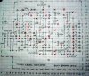
I have made thousands of circuits, some very complicated on "stripboard". It has parallel rows of copper strips and is perforated all over with a 0.1" grid. Each copper strip forms most of the printed wiring of a pcb and the parts and a few jumper wires form the remainder. Each copper strip can be used for many parts of the circuit when it is cut with a drill bit, just deep enough to cut the copper but not make a hole. Every item is soldered to a copper strip.
I plan each circuit layout on grid paper to be as compact as is possible. The red X's are where a copper strip is cut:
Home PCB's generally don't have a silk screen, limited to double sided and no plated thru holes.
HASL (Hot air solder leveling) or plating USUALLY isn't done.
1. Program for generating artwork
Some are free and some with limitations for the free version. Examples: DesignSpark, Eagle, KiCAD
2. Printing of the artwork. The Toner transfer method can only be done with a laser printer. For printing (UV exposure), I like using a polyester translucent paper.
I never tried toner transfer. A clothes iron or modified laminator is typically used in this process ($100). Magazine paper or toner transfer paper is used.
For UV exposure there would be talk about an "exposure frame". I use a drop of water. The UV light source is the other issue. I did a board using sunlight once and a few using a UV source used for photolithography that I had access too. You need to figure out exposure times. The general issues here are is it dark enough.
For the UV exposure you may need a "bug light" and a makeshift darkroom and pre-sensitized PCB's.
I actually made this material, but I had access to an oven and a spin coater.
Etching is very messy and you have to worry about disposal. There are there major chemical systems. Ammonium Persulfate, ferric chloride and hydrogen peroxide/muratic acid.
Etching works better when heated and agitated. Bubbles are sometimes used. Ferric chloride is messy and stains. The hydrogen peroxide/muratic acid is renewable. So goggles, gloves and apron are necessary. Baking soda can be used for neutralization. You need a plastic container to store spent stuff. This is the really messy part.
Another method is isolation milling. You'll need a CNC mill for that.
Drilling. A drill press is almost mandatory. Proxxon is way better than Dremel. PCB drills are carbide and fragile, but you don't have to use them. The runnout on the Dremel is too high. Manual drilling has issues too and solutions.
A camera and laser pointer are two additions.
I've done HASL, but not with air.
Without a silk screen, it's difficult to place components manually. You can do the silk screen process too. It's a UV exposure sort of thing to make the screen and you squeegee the paint through the screen.
You mention 'a PCB' if this is a one-off then I would agree with looking at the strip board option, but for a qty, by the time you have invested in chemicals etc and producing boards without thro hole plating and silk screen it is just as cheap as some of the services out there now, I had a small run of 8"x10" boards done out of China and were very professional and reasonably priced.
Max.
During my electronics career, most products I designed were one-off and the prototype was sold and installed. When I worked for a Japanese PRO audio manufacturer I designed an equalizer for a new speaker using American parts. I got a pcb designed locally and had thousands of circuits made. I designed a sensitive tester for distortion, frequency and levels accuracy and noise. Only two failed, one had its quad opamp IC installed backwards and another had an open capacitor.We sold thousands of ours before the head office Japanese people made their copy of my design using Japanese parts. None failed or were returned.
This site uses cookies to help personalise content, tailor your experience and to keep you logged in if you register.
By continuing to use this site, you are consenting to our use of cookies.
")