I'm experimenting with driving a larger voltage with a uC. I thought I understood how to do this using a darlington pair, but the circuit is not behaving as expected.
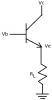
I'll spell out my line of thinking and I'd very much appreciate if someone could explain where I'm going wrong. In the schematic, pin 28 of the uC goes high and allows current to flow into the base of T1 (very low current). A higher current flows through the emitter of T1 and directly into the base of T2. This increases the current gain even more. I believe the collector-emitter voltage drop on a 2n3904 is about 0.3V, so I expected a voltage of 4.2V across Rload.
Instead, I'm getting a collector-emitter voltage drop of 3V across T2, which leaves only 1.5V for the load. Reviewing the datasheet for the 3904s, I don't see that I'm exceeding any capabilities of the transistors. I suspect there's something fundamental I'm not understanding. Thanks in advance for your help.
-Dan
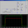
Attachments
Last edited: