Continue to Site

Welcome to our site!

Electro Tech is an online community (with over 170,000 members) who enjoy talking about and building electronic circuits, projects and gadgets. To participate you need to register. Registration is free. Click here to register now.

  • Welcome to our site! Electro Tech is an online community (with over 170,000 members) who enjoy talking about and building electronic circuits, projects and gadgets. To participate you need to register. Registration is free. Click here to register now.

Current Loop Interface Design

Status
Not open for further replies.

Tupinambis

New Member
Greetings,

I am working on my first analog design project which is to build a two-wire current loop interface (preferably 4-20ma) for transmitting the output of an instrumentation amplifier measuring the voltage across a solenoid. An important feature of the project is that the two wires transmit the appropriate interface current and also provide power to the instrumentation circuit and necessary voltage reference. The final design will be used for high temperature applications and that is why I wish to design my own instead of using a commercially available IC.

So far, my setup is the following:
A 2 op-amp (single supply) instrumentation amplifier with referenced
inputs, who's output is represented by V_SIG

A 5V reference used to provide the in-amp reference

A voltage controlled current source driven by V_SIG


I was hoping to use op-amps with low operating currents such that the idle
current (V_SIG = 0V) is lower than 4ma, the additional ~16mA would be
drawn by the VCCS. For testing purposes I have been using a signal
generator to simulate the in-amp output but the rest of the circuit is
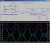
shown below.

Recently, I added the load resistor (used for measuring the interface
current) as shown in the schematic but found that it drastically
attenuated my AC amplitude (1kHz) which was previously 8mA, while the DC level
remained at 12mA. What could explain this behavior?

RESPONSE: Attenuation was due to large bypass capacitance, effectively working with the load resistor as a LPF.

Any additional comments or recommendations are much appreciated since I am
not sure if this is the best approach for designing my interface.

30xipnm.jpg
 
Last edited:
You have just built a great thermometer. Use an IC band-gap Voltage Reference
 
Thank you for the suggestion. The circuit will be exposed to a maximum temperature of ~185° so my choice in commercially available ICs is limited but Digikey has a few options that I will consider.

Concerning the AC signal attenuation, when probing about the circuit I found that with no load resistor the gate voltage of IRF9Z10 had very little to no AC component, increasing the load resistor value produced an increase in this AC component at 1kHz (proportional to V_SIG). I presume this has to do with the oscillating voltage across the load resistor which causes the IRF9Z10's source terminal voltage to drop and OPA1 must compensate for this to maintaing a ~5V reference at the drain terminal. But I don't see how this would explain the attenuation in AC voltage across the load resistor. :confused:
 
What is the desired peak-to-peak amplitude of Vsig?

I assumed +-1V. Here is a prototype Transmitter and Receiver. Note how the all of the current (including the quiescent current of U1) flows through R1. I scaled/offset everything so that the current is 4mA to 20mA as Vsig goes from -1V to +1V; other scaling is possible. The reference voltage in the transmitter is used to center the signal between 4mA and 20mA.

On the receiver, I show how to use a current-to-voltage converter to extract the signal, including offsetting it
 

Attachments

  • D15.jpg
    D15.jpg
    301.3 KB · Views: 203
Last edited:
I have not determined the exact peak-to-peak amplitude of Vsig because it will depend on the the solenoid output voltage and gain-bandwidth product of the temperature rated op/in amplifiers that I can find. But I can say that it will be positive referenced like you have implemented in your design.

This is the circuit surrounding Vsig along with your transmitter/receiver design. I have used 1MΩ resistors to reduce the quiescent current for this part of the circuit but I wonder if it will pose any problems?
30sabti.jpg

Thank you for your detailed response.
 
How much input bias current does your IA need?
Does your IA have inbuilt protection against high voltages (such as the back-emf spike when the solenoid switches off)?
 
The IAs I've found on Digikey/Newark generally have an input bias current less than 100nA. Here is one that I found with +40V input protection.
https://www.ti.com/lit/ds/symlink/ina129-ht.pdf

Regarding the supply ranges, it lists +2.25V to +18V. Does this imply that the lower supply rail must be negative or would it be possible to supply +18V/GND and set the reference pin to +9V to offset the output? I ask this because Digikey lists the supply as being 4.5V ~ 36V, +2.25V to +18V but there is no mention of the former range on the datasheet.
 
+40V input protection.
You will need additional protection against back-emf spikes, so that will probably add to the current drawn.
would it be possible to supply +18V/GND and set the reference pin to +9V to offset the output?
Don't see why not.
 
You will need additional protection against back-emf spikes, so that will probably add to the current drawn.
I will consider this in my final design. EDIT: You were referring to the IA's ESD rating, correct?

Since I would like to design an interface that won't require any negative voltage supply and allows a user to measure the loop current in a conventional manner (through a load resistor in series with the supply), I tested this circuit today and it seems to work well and without the AC attenuation I observed in my previous design. Hopefully it will perform just as well once I combine the reference IC and IA.
33ji7ph.jpg
 
Last edited:
You were referring to the IA's ESD rating, correct?
IIRC the ESD rating quotes a specific energy/voltage/time profile, which is unlikely to be the same as the profile for the back-emf spike, so I don't know how relevant the rating would be to a solenoid switch-off situation.
 
Update

I've revamped my current loop design and it is looking much better today. The janky reference has been replaced with a band-gap reference and I get a decent voltage measurement from R_LOAD which is proportional to the excitation voltage V1.

current_loop_v1.png

The issue now is in increasing the bandwidth of the current loop transmitter while maintaining the appropriate bypass capacitors for my gain and reference ICs, represented by C1 in the above schematic. Since this is a two-wire interface, placing this large bypass capacitor across the power and ground terminals greatly attenuates the signal intended for transmission. I attempted to (naively) isolate, from the signal line, the required bypass capacitances for each IC with a resistor (in a LPF form) but still saw this attenuation.

Reducing the value of C1 increases the bandwidth of the circuit at the cost of introducing more noise to the transmitted signal. Additionally, a bypass capacitance no less than 1uF is suggested for the ICs.

Are there any good methods for isolating the IC bypass caps from the signal line in this way?
 
You can isolate the IC +ve supply with a diode, like this:
LoopMod.gif

BTW, your circuit has Vref and C3 shorted to ground.

Edit: I'm unclear why you have OA1 configured as a Schmitt trigger to square up the sine input and then follow it with the R2C2 filter which will round off the waveform?
 
Last edited:
I will try that out, thank you alec_t.

The short to ground was a mistake, as well as the Schmitt trigger configuration which should have OA1 flipped vertically such that it is an amplifier of the sine input. R2C2 acts as LPF for the amplifier because I get a considerable amount of high frequency noise from the gain stage.

If not from improper bypassing, I suspect that the source of this noise is due to feedback between the sine input (which in reality is a solenoid) and the reference terminal. Ideally, the reference terminal should remain fixed at V_ref, but when probing this point, there is a non-negligible oscillation although it is much more pronounced on V1+ terminal of your schematic. I think this would also explain why the low frequency gain is not exactly 10, since the common mode voltage is not being amplified but it is effectively decreasing the differential voltage seen at V1+.
 
I've tested the diode-isolated circuit and found a particularly interesting problem in this setup.

When the VCCS is at it's lowest current state, the voltage drop across the load resistor is essentially only due to the Q-current of the ICs, at this point the bypass capacitor is charged at Vcc - V_RLoad. As the VCCS current increases, V_RLoad increases, effectively dropping the positive terminal of the diode to a voltage lower than that which the bypass cap is charged with. Here, the diode is "off" and the ICs draw current solely from the capacitor until this voltage is lower than Vcc-V_RLoad. As soon as it is lower (because the VCCS is drawing less current), the diode is "on" and current is drawn from the power supply by the bypass cap.

The result of all this? At VCCS low current, the bypass is charging, increasing V_RLoad when in fact V_RLoad should only be proportional to the VCCS current plus a bias term (Q-current) which must remain constant . In conclusion, this setup does not provide the constant Q-current draw needed for the current loop to function properly.

Can anyone see a way to mitigate this effect while maintaining isolation between the signal path and bypass capacitance?
 
I don't see how you can keep the Q-current constant if you are powering the ICs from the line rather than from a fixed independent source. Line power would involve some sort of charge storage, hence there will inevitably be charging/discharging current superimposed on your VCCS current, as youve already found.
 
Status
Not open for further replies.

Latest threads

New Articles From Microcontroller Tips

Back
Top