Continue to Site

Welcome to our site!

Electro Tech is an online community (with over 170,000 members) who enjoy talking about and building electronic circuits, projects and gadgets. To participate you need to register. Registration is free. Click here to register now.

  • Welcome to our site! Electro Tech is an online community (with over 170,000 members) who enjoy talking about and building electronic circuits, projects and gadgets. To participate you need to register. Registration is free. Click here to register now.

Copper pour "Blobs", what to do with them ?

Status
Not open for further replies.

ItsMike

New Member
Hey everyone,

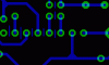
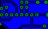
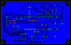
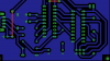
I'm designing a pcb in eagle and I made a copper pour on the bottom layer.
Since I used a rather high isolation (etching at home) I got those copper blobs which do not connect to anything between components/pads ect... (See attachment).

Do I need to get rid of them ? do they have any effect on the circuit ? (parasitic capacitance/noise whatever).
What would be the easiest way of getting rid of them ? I could do that in photoshop since I use it to invert the colors anyways.

Thanks in advance, Mike.
 

Attachments

  • Capture.PNG
    Capture.PNG
    52.1 KB · Views: 463
Last edited:
The isolated blobs are not normally a problem, expect perhaps in RF type circuits. So you can leave them there if you like.
 
Last edited:
Hi,

if you want the blobs to be connected to circuit ground use a trace width of 0.254mm (0.01") and draw a wire from the ground pour into the area you want to fill with a non isolated ground fill.

Name the short piece of wire "ground" (GND) and perform "ratsnest". Ratsnest then connects the blob to circuit ground.

Please refer to the attached five screenshots.

Note the highlighted area. It's all connected to ground. Also note the difference between image4 and 5. Just rerouting of one cap improved the overall ground pour to almost 100%.

Boncuk
 

Attachments

  • blobs-01.gif
    blobs-01.gif
    12.8 KB · Views: 304
  • blobs02.gif
    blobs02.gif
    17.1 KB · Views: 317
  • blobs-03.gif
    blobs-03.gif
    23.6 KB · Views: 280
  • blobs-04.gif
    blobs-04.gif
    25.4 KB · Views: 299
  • blobs-05.gif
    blobs-05.gif
    24.8 KB · Views: 310
Last edited:
The "blobs" are also called "orphans" in Eagle. When you make your polygon, you have the choice of orphans on or off. Try that switch. If you already have the polygon, go to information ("i"), click on the copper filed area, and be sure the orphans box is not checked.

John
 
Last edited:
Thanks a lot.

So it's just aesthetics ? I might as well just turn those "orphans" off without any impact on the circuit, right ?

Also, I've noticed there is a similar option for the polygon - "Thermals" - What does that do ?
 
"Thermals" connect pads to a copper pour by thin connections, i.e., 4 bars between the pad and the copper pour, if the pour completely surrounds the pad. It is done to facilitate soldering. Soldering to a pad in the middle of a copper pour without thermals is more difficult. You cannot turn thermals on or off for specific pads, but there are various workarounds.

John
 
Thanks a lot.

So it's just aesthetics ? I might as well just turn those "orphans" off without any impact on the circuit, right ?

Also, I've noticed there is a similar option for the polygon - "Thermals" - What does that do ?

Hi,

sometimes it might have impact on a circuit, especially working with operational amplifiers at high frequencies. Semiconductor manufacturers recommend signal traces on one layer and a full ground pour on the other one.

Even working with less sensitive circuits using a good ground pour shortens etching time and takes care of equal etching (no under etching of thin traces while etching a big area.)

Last not least etching as little as possible saves etchant and helps to keep a cleaner environment.
 
Status
Not open for further replies.

Latest threads

New Articles From Microcontroller Tips

Back
Top