sakshi.rawal
New Member
Hi there
I'm a complete newbie to LTspice. I have workkes with simulink a bit for circuit simulation but that too was long back.
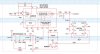
I ahve this circuit to be simulated in LTspice:
**broken link removed**
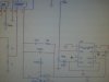
I looked up some tutorials to begin with and when I sat down to work, I realised that the AD8336 is not an available componenet in the LTspice library. Some more search and I came across a .cir file for the AD8336 on the Analog Devices website. So I have managed to create a symbol for the same in the component libraray of LTspice under Auto-generated.
But it doesn't look similar to the one in the circuit or may be I'm not able to interpret it correctly. How do I go about the simulation and adding the components not available alraedy. I'm not even sure if I'm going in the right direction up till now.
If anyone could please help me with this, I shall be highly grateful.
Thanks")
P.S: I have attached an image of the circuit I need to simulate.
Also, I was trying to attach the .cir file, But it says not an allowed extension for uplad. So, I'm pasting the contents of the .cir file here:
---------------------------------------------------------------------AD8336.cir------------------------------------------------------------------------------------------------
*************
* This model was developed for Analog Devices by:
* AEI Systems, LLC
* 5933 W. Century Blvd., Suite 1100
* Los Angeles, California 90045
*
* The model is ©2006, AEi Systems, LLC. All rights reserved.
*
* Users may not directly or indirectly display, re-sell or
* re-distribute this model or any derivative work there from
* without the prior written consent of both AEi Systems and
* Analog Devices. This model is subject to change without
* notice. Neither Analog Devices nor AEi Systems is responsible
* for updating this model.
*
* For more information regarding modeling services, model
* libraries and simulation products, please call AEi Systems
* at (310) 216-1144, or contact AEi Systems by
* email: info@aeng.com. Or visit AEi Systems on the web
* at https://www.AENG.com
*
*Revision B - 8/30/2012*
***
.SUBCKT AD8336 GNEG GPOS INPN INPP PRAO PWRA VCOM VGAI VNEG VOUT VPOS
E_U4_E8 VPBUF 0 TABLE { V(VPOS, 0) }
+ ( (0,0)(2.8,0)(3.0,1.6)(5,3.6)(12,10.6)(15,13.6))·uselim
E_U4_E9 VNBUF 0 TABLE { V(VNEG, 0) }
+ ( (-15,-13.6)(-12,-10.6)(-5,-3.6)(-3.0,-1.6)(-2.8,0)(0,0))·uselim
X_U4_D5 PRAO VPBUF DC_1mV_1A_1V_1nA
C_U4_C3 0 U4_S3 1n
R_U4_R4 0 INPP 450K
C_U4_C5 0 U4_N24227 2.5p
E_U4_E7 U4_N254725 0 VALUE {V(U4_N349891,0)*V(POK,0)}
R_U4_R6 0 INPN 450k
X_U4_D15 VNBUF U4_S3 GEN_DIODE
C_U4_C1 INPN PRAO 2p
X_U4_D13 U4_S3 VPBUF GEN_DIODE
G_U4_G4 0 U4_N24227 U4_S3 0 1
C_U4_C4 INPN 0 6p
X_U4_D6 VNBUF PRAO DC_1mV_1A_1V_1nA
X_U4_S1 PWRAL 0 U4_N254725 U4_S3 PrA_U4_S1
E_U4_E6 U4_N349891 0 INPP INPN 1.0
C_U4_C2 INPP 0 6p
G_U4_G3 U4_N24227 PRAO TABLE { V(U4_N24227, PRAO) }
+ ( (-15,-60m)(-1m,-50m)(0,0)(1m,50m)(15,60m) )·uselim
G_U2_G8 VNEG 0 PWRAL 0 11m
X_U2_U12 VNEG U2_N958367 COMPARATOR2 PARAMS: TH=-2.8
R_U2_R14 0 VNEG 50K
R_U2_R11 0 VPOS 50K
G_U2_G6 VNEG 0 POK 0 14m
X_U2_U16 U2_N968984 POK PWRAL AND
X_U2_U14 U2_N958933 U2_N958855 POK AND
R_U2_R13 0 VNEG 50K
V_U2_V1 U2_AGAINDB1 U2_AGAINDB2 12.04
G_U2_G3 0 U2_AGAINDB1 TABLE { V(VGN, VCOM) }
+ (
+ (-1.0,-14.0)(-0.7,-14.0)(-0.6,-12.5)(-0.52,-9.3)(0.0,17.0)(0.2,27.0)(0.4,37.0)(0.5,42.0)(0.6,46.0)(1.0,46.0)
+ )·uselim
X_U2_D13 GPOS VPOS GEN_DIODE
R_U2_R8 0 U2_AGAINDB1 1
E_U2_E1 VGN 0 GPOS GNEG 1
X_U2_U15 U2_N967091 PWRA U2_N968984 COMPARATOR
G_U2_G7 VPOS 0 PWRAL 0 11m
X_U2_U13 U2_N958367 U2_N958855 INVERTER
E_U2_ABM1 AGAIN 0 VALUE { (10**(V(U2_AGAINDB2)/20))*V(POK) }
R_U2_R12 0 VPOS 50K
C_U2_C5 0 U2_AGAINDB1 20n
X_U2_U11 VPOS U2_N958933 COMPARATOR2 PARAMS: TH=2.8
G_U2_G5 VPOS 0 POK 0 14m
X_U2_D14 VNEG GNEG GEN_DIODE
E_U2_E2 U2_N967091 0 TABLE { V(VPOS, 0) }
+ ( (0,0)(3,0.7) (5,1.2)(12,3.2) )·uselim
X_U2_D16 GNEG VPOS GEN_DIODE
X_U2_D15 VNEG GPOS GEN_DIODE
E_U3_E8 U3_CMOUT U3_N55982 VCOM 0 1
E_U3_ABM1 U3_N62113 0 VALUE { MIN(PWR(V(AGAIN),1),1.6) }
E_U3_E7 U3_N55982 0 TABLE { V(VGN, 0) }
+ (
+ (-0.7,-2m)(-0.6,-4m)(-0.5,-8m)(-0.45,-10m)(-0.4,-14m)(-0.35,-15m)(-0.3,-11m)(-0.25,-9m)(-0.2,-11m)(-0.1,-22m)(0.0,-25m)(0.1,-16m)
+ (0.2,-19m)(0.3,-32m)(0.4,-52m)(0.5,-80m)(0.6,-120m)(0.65,-128m)(0.7,-127m) )·uselim
E_U3_ABM2 U3_N61993 0 VALUE { (V(U3_RIN)-V(U3_ROUT))/nonzero(V(U3_N62113)) }
G_U3_G3 U3_N48981 U3_N48971 TABLE { V(U3_N48981, U3_N48971) }
+ ( (-15,-75m)(-1m,-64.8m)(0,0)(1m,64.8m)(15,75m) )·uselim
X_U3_D16 U3_N48949 VPBUF GEN_DIODE
C_U3_C4 U3_N249674 0 1n
E_U3_E3 U3_N249442 0 U3_N48949 0 1
G_U3_G5 U3_RIN U3_ROUT U3_N61993 0 1
E_U3_E4 U3_RIN 0 VALUE {V(VGAI,0)*V(AGAIN,0)}np
X_U3_D7 VNBUF VOUT DC_1mV_1A_1V_1nA
E_U3_E2 U3_N48981 U3_CMOUT U3_N249674 0 1
R_U3_R15 U3_N249442 U3_N249674 0.1
X_U3_D18 VNBUF VGAI GEN_DIODE
X_U3_D6 VOUT VPBUF DC_1mV_1A_1V_1nA
X_U3_D17 VGAI VPBUF GEN_DIODE
X_U3_S1 PWRAL 0 U3_ROUT U3_N48949 VGA_U3_S1
R_U3_R14 U3_N48971 VOUT 2.5
X_U3_D15 VNBUF U3_N48949 GEN_DIODE
C_U3_C3 0 U3_N48949 1n
.ENDS
.subckt PrA_U4_S1 1 2 3 4
S_U4_S1 3 4 1 2 _U4_S1
RS_U4_S1 1 2 1G
.MODEL _U4_S1 VSWITCH Roff=200 Ron=100 Voff=0.25V Von=0.75V
.ends PrA_U4_S1
.subckt VGA_U3_S1 1 2 3 4
S_U3_S1 3 4 1 2 _U3_S1
RS_U3_S1 1 2 1G
.MODEL _U3_S1 VSWITCH Roff=10 Ron=.001 Voff=0.25V Von=0.75V
.ends VGA_U3_S1
.subckt GEN_DIODE 1 2
D1 1 2 DI2D
.model DI2D D Is=1e-14 Cjo=.1pF Rs=.1
.ends GEN_DIODE
.subckt DC_1mV_1A_1V_1nA A C
G1 A C TABLE { V(A, C) } ( (-1,-1n)(0,0)(1m,1) (2m,10) (3m,1000) )
.ends DC_1mV_1A_1V_1nA
.SUBCKT COMPARATOR2 INP OUT
+ PARAMs: TH=1
EOUT OUT 0 VALUE { IF( V(INP)>TH,1,0) }
.ends COMPARATOR2
.SUBCKT AND A B OUT
EOUT OUT 0 VALUE { IF( V(A)>0.5 & V(B)>0.5,1,0) }
.ends AND
.SUBCKT INVERTER IN OUT
EOUT OUT 0 VALUE { IF( V(IN)<0.5,1,0) }
.ends INVERTER
.SUBCKT COMPARATOR INP INM OUT
EOUT OUT 0 VALUE { IF( V(INP)>V(INM),1,0) }
.ends COMPARATOR
I'm a complete newbie to LTspice. I have workkes with simulink a bit for circuit simulation but that too was long back.
I ahve this circuit to be simulated in LTspice:
**broken link removed**
I looked up some tutorials to begin with and when I sat down to work, I realised that the AD8336 is not an available componenet in the LTspice library. Some more search and I came across a .cir file for the AD8336 on the Analog Devices website. So I have managed to create a symbol for the same in the component libraray of LTspice under Auto-generated.
But it doesn't look similar to the one in the circuit or may be I'm not able to interpret it correctly. How do I go about the simulation and adding the components not available alraedy. I'm not even sure if I'm going in the right direction up till now.
If anyone could please help me with this, I shall be highly grateful.
Thanks
P.S: I have attached an image of the circuit I need to simulate.
Also, I was trying to attach the .cir file, But it says not an allowed extension for uplad. So, I'm pasting the contents of the .cir file here:
---------------------------------------------------------------------AD8336.cir------------------------------------------------------------------------------------------------
*************
* This model was developed for Analog Devices by:
* AEI Systems, LLC
* 5933 W. Century Blvd., Suite 1100
* Los Angeles, California 90045
*
* The model is ©2006, AEi Systems, LLC. All rights reserved.
*
* Users may not directly or indirectly display, re-sell or
* re-distribute this model or any derivative work there from
* without the prior written consent of both AEi Systems and
* Analog Devices. This model is subject to change without
* notice. Neither Analog Devices nor AEi Systems is responsible
* for updating this model.
*
* For more information regarding modeling services, model
* libraries and simulation products, please call AEi Systems
* at (310) 216-1144, or contact AEi Systems by
* email: info@aeng.com. Or visit AEi Systems on the web
* at https://www.AENG.com
*
*Revision B - 8/30/2012*
***
.SUBCKT AD8336 GNEG GPOS INPN INPP PRAO PWRA VCOM VGAI VNEG VOUT VPOS
E_U4_E8 VPBUF 0 TABLE { V(VPOS, 0) }
+ ( (0,0)(2.8,0)(3.0,1.6)(5,3.6)(12,10.6)(15,13.6))·uselim
E_U4_E9 VNBUF 0 TABLE { V(VNEG, 0) }
+ ( (-15,-13.6)(-12,-10.6)(-5,-3.6)(-3.0,-1.6)(-2.8,0)(0,0))·uselim
X_U4_D5 PRAO VPBUF DC_1mV_1A_1V_1nA
C_U4_C3 0 U4_S3 1n
R_U4_R4 0 INPP 450K
C_U4_C5 0 U4_N24227 2.5p
E_U4_E7 U4_N254725 0 VALUE {V(U4_N349891,0)*V(POK,0)}
R_U4_R6 0 INPN 450k
X_U4_D15 VNBUF U4_S3 GEN_DIODE
C_U4_C1 INPN PRAO 2p
X_U4_D13 U4_S3 VPBUF GEN_DIODE
G_U4_G4 0 U4_N24227 U4_S3 0 1
C_U4_C4 INPN 0 6p
X_U4_D6 VNBUF PRAO DC_1mV_1A_1V_1nA
X_U4_S1 PWRAL 0 U4_N254725 U4_S3 PrA_U4_S1
E_U4_E6 U4_N349891 0 INPP INPN 1.0
C_U4_C2 INPP 0 6p
G_U4_G3 U4_N24227 PRAO TABLE { V(U4_N24227, PRAO) }
+ ( (-15,-60m)(-1m,-50m)(0,0)(1m,50m)(15,60m) )·uselim
G_U2_G8 VNEG 0 PWRAL 0 11m
X_U2_U12 VNEG U2_N958367 COMPARATOR2 PARAMS: TH=-2.8
R_U2_R14 0 VNEG 50K
R_U2_R11 0 VPOS 50K
G_U2_G6 VNEG 0 POK 0 14m
X_U2_U16 U2_N968984 POK PWRAL AND
X_U2_U14 U2_N958933 U2_N958855 POK AND
R_U2_R13 0 VNEG 50K
V_U2_V1 U2_AGAINDB1 U2_AGAINDB2 12.04
G_U2_G3 0 U2_AGAINDB1 TABLE { V(VGN, VCOM) }
+ (
+ (-1.0,-14.0)(-0.7,-14.0)(-0.6,-12.5)(-0.52,-9.3)(0.0,17.0)(0.2,27.0)(0.4,37.0)(0.5,42.0)(0.6,46.0)(1.0,46.0)
+ )·uselim
X_U2_D13 GPOS VPOS GEN_DIODE
R_U2_R8 0 U2_AGAINDB1 1
E_U2_E1 VGN 0 GPOS GNEG 1
X_U2_U15 U2_N967091 PWRA U2_N968984 COMPARATOR
G_U2_G7 VPOS 0 PWRAL 0 11m
X_U2_U13 U2_N958367 U2_N958855 INVERTER
E_U2_ABM1 AGAIN 0 VALUE { (10**(V(U2_AGAINDB2)/20))*V(POK) }
R_U2_R12 0 VPOS 50K
C_U2_C5 0 U2_AGAINDB1 20n
X_U2_U11 VPOS U2_N958933 COMPARATOR2 PARAMS: TH=2.8
G_U2_G5 VPOS 0 POK 0 14m
X_U2_D14 VNEG GNEG GEN_DIODE
E_U2_E2 U2_N967091 0 TABLE { V(VPOS, 0) }
+ ( (0,0)(3,0.7) (5,1.2)(12,3.2) )·uselim
X_U2_D16 GNEG VPOS GEN_DIODE
X_U2_D15 VNEG GPOS GEN_DIODE
E_U3_E8 U3_CMOUT U3_N55982 VCOM 0 1
E_U3_ABM1 U3_N62113 0 VALUE { MIN(PWR(V(AGAIN),1),1.6) }
E_U3_E7 U3_N55982 0 TABLE { V(VGN, 0) }
+ (
+ (-0.7,-2m)(-0.6,-4m)(-0.5,-8m)(-0.45,-10m)(-0.4,-14m)(-0.35,-15m)(-0.3,-11m)(-0.25,-9m)(-0.2,-11m)(-0.1,-22m)(0.0,-25m)(0.1,-16m)
+ (0.2,-19m)(0.3,-32m)(0.4,-52m)(0.5,-80m)(0.6,-120m)(0.65,-128m)(0.7,-127m) )·uselim
E_U3_ABM2 U3_N61993 0 VALUE { (V(U3_RIN)-V(U3_ROUT))/nonzero(V(U3_N62113)) }
G_U3_G3 U3_N48981 U3_N48971 TABLE { V(U3_N48981, U3_N48971) }
+ ( (-15,-75m)(-1m,-64.8m)(0,0)(1m,64.8m)(15,75m) )·uselim
X_U3_D16 U3_N48949 VPBUF GEN_DIODE
C_U3_C4 U3_N249674 0 1n
E_U3_E3 U3_N249442 0 U3_N48949 0 1
G_U3_G5 U3_RIN U3_ROUT U3_N61993 0 1
E_U3_E4 U3_RIN 0 VALUE {V(VGAI,0)*V(AGAIN,0)}np
X_U3_D7 VNBUF VOUT DC_1mV_1A_1V_1nA
E_U3_E2 U3_N48981 U3_CMOUT U3_N249674 0 1
R_U3_R15 U3_N249442 U3_N249674 0.1
X_U3_D18 VNBUF VGAI GEN_DIODE
X_U3_D6 VOUT VPBUF DC_1mV_1A_1V_1nA
X_U3_D17 VGAI VPBUF GEN_DIODE
X_U3_S1 PWRAL 0 U3_ROUT U3_N48949 VGA_U3_S1
R_U3_R14 U3_N48971 VOUT 2.5
X_U3_D15 VNBUF U3_N48949 GEN_DIODE
C_U3_C3 0 U3_N48949 1n
.ENDS
.subckt PrA_U4_S1 1 2 3 4
S_U4_S1 3 4 1 2 _U4_S1
RS_U4_S1 1 2 1G
.MODEL _U4_S1 VSWITCH Roff=200 Ron=100 Voff=0.25V Von=0.75V
.ends PrA_U4_S1
.subckt VGA_U3_S1 1 2 3 4
S_U3_S1 3 4 1 2 _U3_S1
RS_U3_S1 1 2 1G
.MODEL _U3_S1 VSWITCH Roff=10 Ron=.001 Voff=0.25V Von=0.75V
.ends VGA_U3_S1
.subckt GEN_DIODE 1 2
D1 1 2 DI2D
.model DI2D D Is=1e-14 Cjo=.1pF Rs=.1
.ends GEN_DIODE
.subckt DC_1mV_1A_1V_1nA A C
G1 A C TABLE { V(A, C) } ( (-1,-1n)(0,0)(1m,1) (2m,10) (3m,1000) )
.ends DC_1mV_1A_1V_1nA
.SUBCKT COMPARATOR2 INP OUT
+ PARAMs: TH=1
EOUT OUT 0 VALUE { IF( V(INP)>TH,1,0) }
.ends COMPARATOR2
.SUBCKT AND A B OUT
EOUT OUT 0 VALUE { IF( V(A)>0.5 & V(B)>0.5,1,0) }
.ends AND
.SUBCKT INVERTER IN OUT
EOUT OUT 0 VALUE { IF( V(IN)<0.5,1,0) }
.ends INVERTER
.SUBCKT COMPARATOR INP INM OUT
EOUT OUT 0 VALUE { IF( V(INP)>V(INM),1,0) }
.ends COMPARATOR