Continue to Site

Welcome to our site!

Electro Tech is an online community (with over 170,000 members) who enjoy talking about and building electronic circuits, projects and gadgets. To participate you need to register. Registration is free. Click here to register now.

  • Welcome to our site! Electro Tech is an online community (with over 170,000 members) who enjoy talking about and building electronic circuits, projects and gadgets. To participate you need to register. Registration is free. Click here to register now.

Chess Circuit Project HELP!

Status
Not open for further replies.

Canyouknott

Member
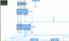
I have an assignment to explain how my Chess timer actually works... Will anyone be able to help me explain or corrert me with anything and also suggest option which I should include in the following 'Word document'...

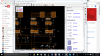
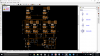
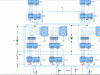
THe criteria of this assignment was to explain the processes which are happening in this circuit


THANKS in advance to anyone who helps :)
 

Attachments

  • Stage 1 Elec Major Project Investigation.doc
    860.5 KB · Views: 258
The 4510 counts on the positive-going edge of the clock input. Normally a counter counts when the input button is pressed, but all of your circuits count when the button is released. Why?

The 4510 has carry logic built in, and the datasheet shows how to connect parts as a multi-digit counter. Why did you do something different?

ak
 
I have seen the datasheets and can not see an explanation to do so concerning the carry logic... This circuit was originally going to be used with a different IC such as a 4553B but due to have a simulating software which does not include this particular IC (For some apparent reason) I could not do so.

And about the input when button is released, I could not find a way to 'not' do this without including an schmitt NAND gate within the circuit... It was required that I did so that is way :)
 
And about the input when button is released, I could not find a way to 'not' do this without including an schmitt NAND gate within the circuit... It was required that I did so that is way :)

The "pulse" button goes through two transient suppression diodes (why, when the other two button inputs are not protected?) to a NAND gate that is acting as an inverter. To get the counter to count on the leading edge, bypass this inverter and connect the pulse button directly to the next gate, the one that also is driven by the flipflop.

Note that this discussion would be much easier if *every* component has a unique reference designator.

ak
 
upload_2015-10-13_9-6-8.png

Oh I see what you mean... Like this (carry)
 

Attachments

  • upload_2015-10-13_9-5-39.png
    upload_2015-10-13_9-5-39.png
    208.1 KB · Views: 205
Oh I see what you mean... Like this (carry)

I pointed this out to you in your other thread.

Also I stated the importance of not leaving CMOS inputs 'floating' ie: disconnected. example the 4510 PL is still open.!
 
What do you mean by CMOS and where is the 4510 PL?

Hi,
If you check the datasheet for the 4510 it explains that the device is CMOS technology.
This means that the Input pins of the IC have a VERY high input impedance [resistance].

If left unconnected the input pin can assume a High or Low state depending upon the local electrical fields on the PCB [ or You!]
You can image what effect this would have if the Pload drifted High and Low, it could keep loading the 4510 with what ever state the 4 parallel inputs are at that instant.

If you do not use a CMOS input pin, connect it High or Low to suit the required operation of the IC. OK.?


PL = Load = Parallel Load [pin #1 on the 4510]

E
 
Last edited:
So Pin 1 on the 4510B has to be LOW?

Are there any other errors on my ciruit relating to that CMOS stuff...? Like the clock pin., do I have to have that 10k resistor connect to 9Vs there?, sorry datasheets are very confusing for me at the moment
 
upload_2015-10-13_21-39-18.png

On this mode selection table it says PL has to be LOW for a count up or down decade, Correct? And there is a 'CE' abbreviation which has to be LOW, what is that?
 
First - I'm not picking on you, but it is clear from your questions that you are a bit unprepared for the level of circuit design you are attempting.

If you are doing logic circuit design with real-world parts, there are some concepts you have to know before starting if you want to have any chance of success. I'm surprised and disappointed in your teacher that these concepts have not been taught before the start of this project.

Any pin that is an input must have a defined condition. Determining which pins are inputs comes from reading the datasheet. Knowing how to stabilize these inputs comes from instruction and guidance. This forum is here to help, and we certainly have the horsepower to guide you through this project, but it would be much more efficient to get it in the classroom - unless the true nature of the project is to toss you into the pool and see if you can swim on your own. If so, I think this project is a bit too complex for such a scheme. But, onward...

I suggest that you read the Wikipedia page on CMOS. You can skip the device physics stuff (unless that's what excites you), but go through the tech details, logic, and dissipation parts to get a feel for how CMOS functions. Some of it won't make much sense yet but it will eventually, and it always helps to know how your parts think inside. Then make a table for the 4510 listing every pin. For each one, determine if it is an input or output. For each input, determine how it should be treated. Some are easy, such as the clock input - you handle it by driving it with a clock signal. Think through every pin, then adjust the schematic. Using a new part always is tricky, even for experienced designers. It takes discipline to make sure you've captured every little quirk.

ak
 
hi Can,
This extract from the 4510 d/s explains the operation of the PL pin, also pins P0, thru P3 for the data inputs that will be loaded.

As post #12 suggests ,, get to know your datasheet data, it will save you hours of aggro.

E
 

Attachments

  • AAesp01.gif
    AAesp01.gif
    38 KB · Views: 187
First - I'm not picking on you, but it is clear from your questions that you are a bit unprepared for the level of circuit design you are attempting.

If you are doing logic circuit design with real-world parts, there are some concepts you have to know before starting if you want to have any chance of success. I'm surprised and disappointed in your teacher that these concepts have not been taught before the start of this project.

Any pin that is an input must have a defined condition. Determining which pins are inputs comes from reading the datasheet. Knowing how to stabilize these inputs comes from instruction and guidance. This forum is here to help, and we certainly have the horsepower to guide you through this project, but it would be much more efficient to get it in the classroom - unless the true nature of the project is to toss you into the pool and see if you can swim on your own. If so, I think this project is a bit too complex for such a scheme. But, onward...

I suggest that you read the Wikipedia page on CMOS. You can skip the device physics stuff (unless that's what excites you), but go through the tech details, logic, and dissipation parts to get a feel for how CMOS functions. Some of it won't make much sense yet but it will eventually, and it always helps to know how your parts think inside. Then make a table for the 4510 listing every pin. For each one, determine if it is an input or output. For each input, determine how it should be treated. Some are easy, such as the clock input - you handle it by driving it with a clock signal. Think through every pin, then adjust the schematic. Using a new part always is tricky, even for experienced designers. It takes discipline to make sure you've captured every little quirk.

ak
At school I'm about 2 weeks ahead of my whole class. This project was recommended by my teacher to be done in year 12, but I believe I can learn alot if I start now. I might not know the critical aspects of this project but that's why I found this forum. It has helped me improve in alot of aspects in electronics. My teacher has explained truths tables of these logic ICs and that's about it :) Of coarse I don't know that much about logic but the one and ONLY way is to learn and try.. :) I feel I have made alot of progress, but of coarse there are improvments to be made. When year 12 hits me I will have won half the battle because logic gates etc are the main focus in year 12

Thanks
 
So basically concerning the 4510B. It is CMOS technology therefore it's sensitive to electro field which can alter the state of inputs???? The Load pin must be connected to 0V as well as Load1 and LOad8. But Load 2 and 4 must be connect to HIGH... correct? All inputs must be connect to a state right?
 
hi C.
The 4510 IC has a parallel load option, this means the internal counter can be preloaded with a count value.
The P3,P2,P1,P0 are 'weighted' as 8,4,2,1 , this means that if P3 is High and P2,1,0 are Low when the Pload pin is High, the internal counter will be set to a numeric value of '8'.

You would then set PL Low, so on the next Up clock count the counter would increment to 9 or if you down counted the counter would decrement to 7.

So by correctly setting P3,2,1,0 to a required value and using PL the counter can be preset.

OK.?
E
 
upload_2015-10-17_15-29-58.png

Could you just tell me if this is correct... It seems to be you're answers are just too over complicated.. I only need a yes or.... no
 
upload_2015-10-17_16-18-26.png

upload_2015-10-17_16-18-47.png


upload_2015-10-17_16-19-43.png

Is this pi configurations correct, now?????
I have added anew button which pulses when pushed to both players first display... e.gPlayer 1, 899 secs and PLayer 2 455 secs. Button pressed now 799 and 355. (Depending on state of Up/down input as well
 

Attachments

  • upload_2015-10-17_16-16-30.png
    upload_2015-10-17_16-16-30.png
    110.4 KB · Views: 185
Could you just tell me if this is correct... It seems to be you're answers are just too over complicated.. I only need a yes or.... no

Answer, Yes/No is not the way to understand a circuit
upload_2015-10-17_8-36-51.png

So basically concerning the 4510B. It is CMOS technology therefore it's sensitive to electro field which can alter the state of inputs???? The Load pin [ do you mean Pload ] must be connected to 0V as well as Load1 and LOad8.[ there is no Load 8 pin] But Load 2 and 4 must be connect to HIGH... correct? All inputs must be connect to a state right?
The Load pins L3,2,1,0 are 'weighted' 8,4,2,1 [ look up 'weighting]

Ask yourself what parallel Load means.? If you are not preloading the counter by the use of Pload, WHY would you want to Set L2 and L4, High.???

E

Added images
 

Attachments

  • AAesp02.gif
    AAesp02.gif
    19 KB · Views: 201
  • AAesp03.gif
    AAesp03.gif
    27.5 KB · Views: 213
Last edited:
Use this image this 4510 diagram for our posts so that we are using the same terminology.

upload_2015-10-17_8-58-54.png
 
Status
Not open for further replies.

Latest threads

Back
Top