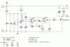
I'm trying to build and fully understand the functioning of Mr. Chemelec's dump charger circuit. Below is the circuit and what I understand of it. Any corrections of my explanation would be greatly appreciated! Also, we want a pulse width modulation into the circuit to keep the battery fully charged when the solar panel is charging. Any ideas on how this can be done?
Circuit
**broken link removed**
My explanation of the circuit
Circuit Operation
LEDS
1. If LED2 is lit up and NAND2 produces a logic 0, the transistor is off.
A. If LED1 is lit up and NAND2 produces a logic 1 the transistor is saturated. Thus, the P-MOS is active and the battery is charging.
2. If LED 1 is it up and NAND3 produces a logic 0 the P-Mos is off, therefore no current can flow to the main load. Also, if the P-MOS is off current is forced to charge the battery.
A. When LED1 is off NAND3 produces a logic 1 and the P-MOS is turned on. Therefore, the main load draws current.
Dual Comparators
The explanation above is the normal functioning of the circuit. The dual comparators are used to regulate the normal functioning of the circuit. By using 2, 10k Potentiometers (VR1 & VR2) the amount of resistance can be varied. This resistance can be converted to voltage a level.
1. For VR1 the voltage at which the P-MOS will go high and the battery will begin to charge is set.
A. For the P-MOS to go high, comparator 1 switches from a logic 1 to 0 output. The output is then run through NAND 2 and becomes a logic 1 output. The result is the P-MOS and transistor both turn on or go high and the N-MOS controlling the dump load goes low or turns off. Once the battery voltage has returned to the set level the steps above will reverse or return to their original state.
2. VR2 is the voltage at which the P-MOS will go low and the main load will be disconnected from the circuit.
A. For the P-MOS to go high, comparator 2 switches from a logic 1 to 0 output. The output is then run through NAND3 and produces a logic level low or 0. The result is the P-MOS turns off and the main load is disconnected from the circuit.
• 470 micro farad capacitor attached across the positive and negative rails to act as a smoothing capacitor; Absorbs voltage spikes etc.
• .1 Farad capacitors function as smoothing capacitors for the LM393 chip and CD4011 chip.
• P-MOS and N-MOS gates function as digital relays. For the N-MOS the gate voltage threshold is below 1.5 volts and no current will flow through the drain to source. When the gate voltage is above the threshold current flows through the drain to source. When the gate and drain voltage is significantly high the N-MOS is in saturation allowing maximum current flow through the component. For the P-MOS no current flows unless the gate voltage is lower than the drain voltage by 1.5 volts. When the threshold is met current flows through the source to drain. If the gate and drain voltages are significantly low the P-MOS is in saturation and current flow is at maximum through the source to drain.
• D2 and D3 function as bypass capacitors and minimize leakage current from the battery.
• Positive feedback resistors for the LM393 provide hysteresis, disconnecting the main load for a period of time and allowing the battery to charge during that period.