Continue to Site

Welcome to our site!

Electro Tech is an online community (with over 170,000 members) who enjoy talking about and building electronic circuits, projects and gadgets. To participate you need to register. Registration is free. Click here to register now.

  • Welcome to our site! Electro Tech is an online community (with over 170,000 members) who enjoy talking about and building electronic circuits, projects and gadgets. To participate you need to register. Registration is free. Click here to register now.

Certain questions about FAN7392N High and Low side gate driver

Status
Not open for further replies.

Right_Then

New Member
Dear Fellows,

i am having trouble getting the output on the HO pin of this device. i am using arbitrary components to test this IC but to no avail.

Few clarifications required are as such please

1) For low-side the power supply`s positive is supposed to be connected to the Vcc (pin no 3)
then would it be okay to connect the negative of that supply to COM (pin number 2).

2) For IC power i am connecting +ve to (Pin 9) Vdd and -ve to (Pin 13) Vss.

3) i am assuming that internally the IC itself isolates these two supplies so grounds of these
two supplies dont become one but remain separated is that true? if that is not the case then
did the scheme presented in the datasheet is actually referring to the same supply but at two
places to avoid drawing extra lines.

4) Signals supplied to Pins 10,11,12 (HIN,SD,LIN) from micro-controller side need not be isolated
with Optocoupler since this side of IC is internally isolated anyway from the High and low side
supplies?? is that correct assumption?

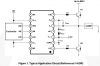
the scheme that is given in the datasheet. i etched it. that scheme and the one presented in the datasheet is provided as attachments. Please have a look if i interpreted it correctly or not.


Thanks
Regards
 

Attachments

  • fan7392nDcircuit.png
    fan7392nDcircuit.png
    18.9 KB · Views: 673
  • FAN7392N_6 - PCB.pdf
    102 KB · Views: 249
deleted
 
Last edited:
1) For low-side the power supply`s positive is supposed to be connected to the Vcc (pin no 3)
then would it be okay to connect the negative of that supply to COM (pin number 2).
The return for Vcc (pin 3) is COM (pin2). This is the low-side supply that determines the output swing of the low-side output. The low-side supply would be connected between Vcc (pin3) and COM (pin2).

A separate logic-supply is used to define the expected input logic swing of the logic inputs, say 5V. A 5V supply would be connected between Vdd(pin 9) and Vss (pin13).
Vss (pin 13) would usually be jumpered to COM(2), but they are kept separate to minimize ground-loops.

2) For IC power i am connecting +ve to (Pin 9) Vdd and -ve to (Pin 13) Vss.
see above

3) i am assuming that internally the IC itself isolates these two supplies so grounds of these
two supplies dont become one but remain separated is that true? if that is not the case then
did the scheme presented in the datasheet is actually referring to the same supply but at two
places to avoid drawing extra lines.
Only for testing. In actual application, there would be three supplies; a 5V logic supply, a 15V supply for the low-side driver (these two could share a common), and a floating 15V high-side (Vb and Vs) supply that could sit at +585V with respect to the other two...

4) Signals supplied to Pins 10,11,12 (HIN,SD,LIN) from micro-controller side need not be isolated
with Optocoupler since this side of IC is internally isolated anyway from the High and low side
supplies?? is that correct assumption?...

See above.
 
Last edited:
Thanks MikeMl for replying

I was just trying to confirm that i had not assumed it wrong to consider which is +ve and -ve on this IC.
it is exactly how you have mentioned that i have connected the IC. Also i am using three separate supplies.
regarding the floating part. it is my understanding that if two power supplies don't share a common negative then they might be floating
with respect to each-other. like a 9v battery on my table and adjustable power supply which is rectifying from mains are floating with respect to each-other.
or is it a wrong assumption?

if what i am assuming is right then how come even if i use two different supplies for high-side gate and low-side gate which ultimately draw their power from mains be considered floating.( although they are coming from two different/independent apparatus/devices ). Only reason to think of them as floating with respect to each-other would be that they both have transformers isolating them from mains. then would that mean every time i need a floating supply with respect to each other i can use transformer between them and then it is game. Or does floating here mean a wire connected to +ve but has not reached any -ve yet.

i am asking it this minutely because if i have done identical to what you have said above then why is there no output atall.


Thanks
Regards
 
Transformer based power supplies provide isolation between the Line side and the output side up to the breakdown voltage of the insulation between windings, usually >1000V, but limited to 2 to 3kV. This also applies to two or more isolated windings on the same transformer core.

You can determine if two supplies are isolated by connecting an Ohmmeter between their negative outputs. ZeroΩ means they are not-isolated, or cross connected through the external wiring.

Did you read this app note?
 
Status
Not open for further replies.

Latest threads

Back
Top