Continue to Site

Welcome to our site!

Electro Tech is an online community (with over 170,000 members) who enjoy talking about and building electronic circuits, projects and gadgets. To participate you need to register. Registration is free. Click here to register now.

  • Welcome to our site! Electro Tech is an online community (with over 170,000 members) who enjoy talking about and building electronic circuits, projects and gadgets. To participate you need to register. Registration is free. Click here to register now.

CC/CV digitally controlled power supply

Status
Not open for further replies.

Gobbledok

Active Member
Hi guys I am in the process of making a constant current/constant voltage power supply controlled by a STM32F4 with a colour LCD touch screen.

I have already designed and made the control board and most other parts of the power supply and now I'm in the process of designing the high current output circuit. I am more of a digital person rather than analog and this is where I require the expertise of people smarter than I :)

Attached is what I have designed however due to my limited experience with analog electronics I don't know if this is a good way to do it. As far as I know I may have broken several cardinal sins and not even know it, however I am pretty sure it will work (to a degree).

I apologise for the 'old fashioned' schematic but we work with what we have :)
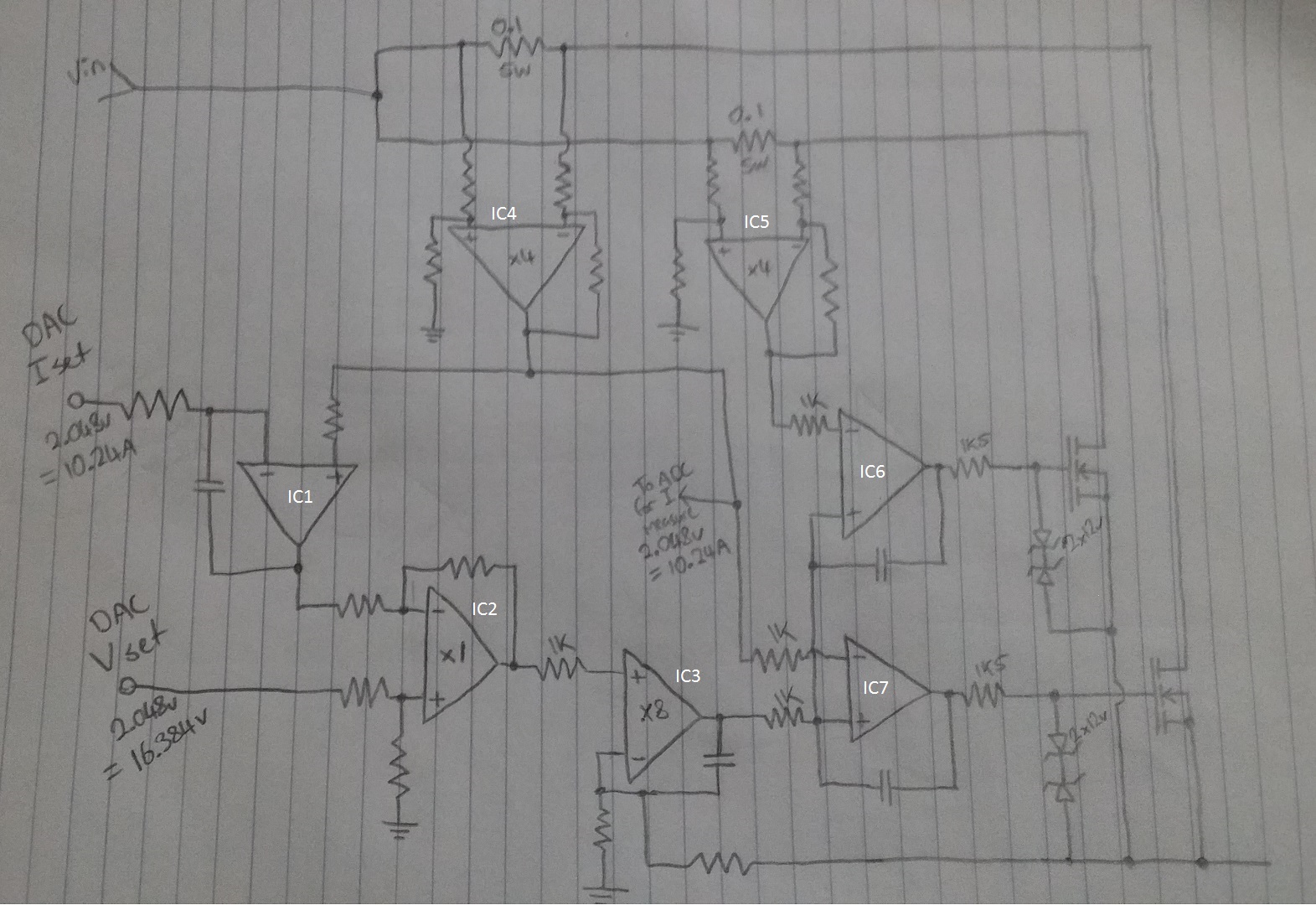
Output Schematic.jpg


I forgot to write it on the schematic but the output is in the lower right of picture (obviously). In the final unit there will be 2 of these in parallel for 20A output. The current sharing between each will be done in software.

The gains will all be set manually (calibrated) with 25 turn trimpots, this is why I haven't added resistor values.

The DAC's are 12 bit (MCP4922) and have a precision, low noise 2.048v reference. The op-amps (AD822AN) are rail-to-rail but will likely be run from a -5v/+25v rails. The output MOSFETs are Exicon 10N20.

Please make any suggestions you can think of and if you need any more information please ask.
 
Last edited:
The bottom-left opamp seems to be comparing apples and oranges, since it has a current-dependent input and a voltage-dependent input? The output voltage of your supply will therefore depend on the current the load draws. Is that your intention?
You will need massive heatsinks for the output FETs ;).
 
I re-uploaded the schematic with some labels to make it easier to discuss.

My thinking is:
Lets say that it is in constant voltage mode and the output of IC1 is zero. IC2 will amplify the difference between the output of IC1 and the DAC Vset voltage. While IC1's output is 0, then it will function as a follower until the Iset voltage is exceeded. Once this happens, IC1 will increase its output and therefore lowering the output of IC2 until the current limit is no longer exceeded.

IC3 should be regulating the output voltage with its negative feedback. It should give the correct voltage to IC6 and IC7 to keep the output voltage at the setting. IC6 and IC7 make sure that the current is shared between each MOSFET pair.

I understand that it can't regulate the output voltage with 0 output current. I may have to put a high value resistor on the output to make sure there is always some output current.

I'm still learning though but that is my thinking on what it does.

BTW I have a massive fan forced heatsink, 0.3°C/W rating :)
 
You need to calculate some real resistor values. You would have a really hard time adjusting so many trimpots in any sane way. Not to mention they are expensive.

I am inclined to worry about your dual paths of feeding input to your dual mosfets, A single current sensing resistor, amp and driver chain would be easier to understand and (more importantly) less to go wrong. Your dual path is inherently un-balanced since only one of the sense amps is in the control loop. You might be able to set it up perfectly to start with, but with half your output circuit out of the V/I setting loop, you are bound to have problems.

But don't pay too much attention to me, I don't know much ;)
 
Hi thanks for your thoughts.

I don't mind spending a couple of hours calibrating it all once it is set up. It will be easy enough to disable nodes and calibrate it all separately. I already have the trimpots so the cost isn't a factor. If however trimpots have a worse temperature coefficient, or some other issue I would have to consider.

As far as the current sharing goes, IC6 and IC7 control the current in each MOSFET, and both of those have a single input, being the output of IC3. If they are doing their job properly, then the current should be the same through each sense resistor, and I should have to only measure one for the current limiting.

Maybe I would be better off eliminating IC1 and IC2 and doing current limiting in software? I don't think this would have the same performance though.

I have made some changes to the original schematic, mainly for neatness but also to fix an error with the non-inverting input of IC6. Once again I apologise for the primitive schematic.

Output Schematic.jpg


Also, here's what I have so far:

Power Supply.jpg


So far I have just done the basic power supplies and the control board. For the front I have a 5" 800 * 480 touch screen. The board is an STM32F4 from ebay. It has 1MB of SRAM, 128MB of NAND flash and 16MB of NOR.

It has a DS1302 onboard for timekeeping and a bit of battery backed RAM. I am controlling the fans with a linear voltage and measuring the RPM also. It will have temperature sensors on the 5v regulator, the main bridge rectifier, the output MOSFETs and/or the heatsink.

Total overkill for a power supply but most of this stuff I had laying around and decided to put it to a practical use.
 
Last edited:
I also have a few more questions:

1. How do I calculate the required capacitance? The DC voltage should be (15 x sqrt(2) - diode voltage drop) ~19.8V.

2. Related to the question above. What overhead voltage do I need? I want to be able to output up to 15V regulated. Disregarding ripple voltage, is the output voltage only limited by the gate voltage? Therefore as long as I can supply enough gate voltage to the MOSFETs, then I can output 15V with only 15V (+ the current sense resistor voltage drop) in? I wish to know my allowed ripple voltage. Edit: I would like up to 20A output but can limit the current at perhaps 15A at higher voltages if I have to. The transformer is 300VA 15V.

3. What value capacitors should I have from the output to the inverting input of the op amps? I think if I go too large it will effect the response time of the power supply, but if they are too small it may oscillate?

4. Should I put some resistor feedback on IC1 to limit the gain, or is the feedback from the current sensor enough? I am worried that it will oscillate or produce ripple when it goes into current limit mode. I don't really understand phase shift but I think it will play a part in its feedback.

5. I would like to put an n-channel from the non-inverting input of IC6 pull it to ground with the MCU which would allow me to disable that node at lower current levels and double the current sense resolution. I would also increase the value of the 1K resistor to compensate. Is there a problem with doing that?
 
Last edited:
Rather than try to inform you from my limited knowledge, here is a useful link:
https://www.electro-tech-online.com/threads/power-supply-design-for-beginners.113613/

I did read recently that despite appearances to the contrary, in a linear psu with a more convention layout (ie, pass element is an emitter follower driven by an emitter follower, you actually need about 3 volts more rms than your highest dc output. Even with a low dropout design, which yours appears to be, you still need some headroom as this will give you further ripple reduction. So you should probably have an 18v transformer. But I've learnt something here - I never knew 1.4142 was the square root of 2! I always just used it as a magic number :)

There is a surprisingly effective design to address ripple posted on here recently, hard to make sense of (looks bonkers to be honest) but well worth a look: https://www.electro-tech-online.com...sperate-measures-with-my-power-supply.141942/ - further along the thread contributors have done some simulations.

Speaking of simulations, why not try simulating the analogue aspects of your design. LTSpice is a favourite here, TinaTI is good also.

Sorry I don't know much about mosfets to answer point 2 - but I think I gave you a partial answer above.

Re point 3 - I'm pretty ignorant when it comes to op-amp design, but the simplest thing to do would be to find out the impedance you need to get the feedback you want at the frequency you are interested in, and choose your caps based on that. While I think of it, since you are interested in fast reaction times, your "big slow" here is going to be the rc network formed by the 1k5 resistors, the zener junction capacitance and the mosfet gate capacitance. Whilst on the subject, be careful about what kind of load your opamps IC6 and IC7 can handle with regards to capacitance, though the resistors should make it a non-issue in the majority of devices.

4 - Depends on the feedback path through the ADC and DAC. Chances are you need to lower its gain, possibly even down to unity. But then you say "goes into current limit mode" - so this is supposed to be a limiting circuit, not a constant current setting? Better as it is then, but I don't think it is going to do what you want.

6 - I may be wrong but I think you are missing an important point in all of this - the tolerance of your two 0.1 ohm resistors. Consider if one out by +5% and the other by -5%. This is going to be considerably worse than the resolution of you DAC/ADC combo. So when you use just one of them for something, you create an intrinsic error. That's okay for your load sharing scheme as it is, you can just calibrate it out, but when you talk about using just one to get double the resolution, it's a false economy - the calibration for 2 sense resistors become irrelevant.

I don't see any path to tell the micro what the output voltage is. Without this your high resolution voltage setting is meaningless, trimpots or not. Suppose you set it up so 5.000v setting = 5.000v output. You run it for a week. During this time, all the voltage references will have drifted, the mosfets will have drifted, the resistors and trimpots may have drifted, the opamps won't have the exact same characteristics they did. Oh I forgot, you also have thermal effects whilst it is running, including emf's due to all the soldered joints, drift in the voltage references, drift in all other semiconductors, drift in the resistors, probably worse in the trimpots unless they are low tempco. These effects might cancel out, or they might add up. You only have limited voltage feedback (via IC3 AFAICT) to compensate for drift in the mosfets.

That's some impressive kit you have there, BTW. What are the blue and brown things?

Well, hope this helps.
 
Last edited:
Hi throbscottle thanks for your reply, very helpful.

Regarding LTSpice, I have used it in the past a little bit, maybe now I should get into it a bit more.

With regard to gate capacitance, would that be "input capacitance" in the data sheet?
Untitled.png
Would it be better to buffer the gate voltage after the zeners and use maybe a 100R resistor instead? The op-amps I am using can drive a 350pf load but the mosfet input capacitance (I think that would be the gate) is around 500-700pf. Will the 100R resistor help? Will this only affect the dynamic characteristics?

For the current, when it reaches the limit set by the DAC, it should go into constant current mode. If I lower the gain of IC1 to unity, I'm not sure but I don't think it will be able to supply enough output voltage to lower the output of IC2 and reduce/regulate the current under some conditions.

Hopefully I should be able to tune out the resistor error by calibrating the gain of IC4 & 5. When I talk about double the resolution, I mean when I disable IC6 and its associated mosfet. In that case 2.048V output would equal 5.12A. You are correct though, when both mosfets are enable it doesn't work that way. I think I should try breadboarding it and see how hard it is to calibrate the sense resistors.

I will be dividing and buffering the output voltage as well so I can read it via ADC and correct for errors to a certain degree.

I am not really worried about absolute precision (0.001V) accuracy of the voltage output. I think .1 of a volt would be enough. For the current perhaps 50mA accuracy would be good but I don't know if this is attainable. The constant current would come in handy for testing LED's and such. With only 1 mosfet enabled 50mA will have a count of 40 on the ADC but I'm not quite sure how accurate it will all be.

When you are talking about drifts and such, what sort of percentage are we talking? Is the any way to calculate this or is it a try it and see sort of thing? I am reading the output voltage though so should be able to correct for voltage drift. I don't know about drift in the current sense circuit though. I would really like to avoid using a third current sense resistor if I can avoid it. I don't think I can remove the 2 I have.
Do trimpots drift over time or with temperature? It wouldn't matter if the total value of the trimpot varied, as long as the percentage remained the same I guess.

They're potted pcb mount toroidals. Because of what I had laying around I have a transformer for the fans, a transformer for the 5v supply, and a transformer for the op-amp supply.
 
Last edited:
I have updated the schematic to show the mosfet which disables IC6, and added gate buffers after the zeners.
Output Schematic.jpg
 
I have a few comments and resources:

The first resource is the https://www.google.com/url?sa=t&rct...ostw0n7h4A9KnhRatyomXZA&bvm=bv.73612305,d.aWw one.

You had mentioned paralleling power supplies. There is some info in the above document. When paralleling, one supply acts as a voltage source and the other as a current source generally with the compliance equal to the regulated voltage when they act as a voltage source.

You also asked about filter caps. One "rule of thumb" is 1000 uF/amp minimum.

You might consider usinf a high side current sense amplifer.
 
Everything drifts over time, semiconductors more so. You probably wouldn't notice it with passive components. For the level of accuracy you are talking about though it doesn't sound like you need to worry about it. Good to be aware though.
Yes, input capacitance.
I forgot to ask in previous post - why have you got back to back zeners between g and s of the mosfets? afaict, all they do is contribute noise to the output.
You really ought to consider driving your mosfets with bipolar transistors.
If you have one of your trimpots connected as a rheostat, think about what will happen to the set value if the overall resistance changes.
You really ought to be aiming for at least 10mA resolution with your current setting, and better than 0.1v resolution with the voltage, to do justice to that nice display and mcu.
You can get some degree of adjustment for the sense resistors by connecting a pot across the one with the highest value and reading the voltage between it's wiper and one end. Of course this is going to create a small offset due to the input impedance of its diff amp - something you will need to calculate to find out the effects.
 
I kinda like that case. Was it part of your junkbox or do you know the company that made it?

Aside:
I made a lot of stuff at work and used the LMB Heeger Unipac rack enclosures. **broken link removed** They are made with basically with six panels and nor supports. The front and rear panels are bent to integrate the top and bottom supports and they used clinch nuts to put everything together.

I didn't like the aesthetics of the rack handles as an extended side, so I used real ones. I never had any reason to use the chassis, although for one piece I should have with a cutout on the chassis to expose the back of the PCB.

Many times I would use slides. In a few cases I used magnetic catches for the lids. In one case I made the back totally open with two 1/4" bars across the back.
That case was used as a "splitter" so to speak. It brought in instrument cables which were attached to the rods with tywraps. Inside were DIN rail sockets to screw terminals.
This way, I was able to bring in the instrumentation and "split" it to the D/A, A/D and digital boards.

Unfortunately, I was overruled when I wanted a separate acquisition system (single connection to PC) and not cards which turned out to be a mistake.

I essentially made reusable, reconfigurable instrumentation, but nothing got reused in my lifetime there.

==

With high current output, you should also be considering sense leads.
 
throbscottle thanks again for your thoughts.

The zeners are there to keep the G-S voltage within acceptable limits. I didn't think about the added noise though but I don't think it will be too much of a problem because the signal/noise ratio will be very high.

If I use transistors on the gate, would I need a transistor high and low? I am guessing I need to turn it off as fast as I turn it on?

Thanks for your suggestions, I wanted to be more optimistic for my accuracy and wasn't sure what sort of accuracy was attainable and will now aim a bit higher.

KISS thanks for the link and your thoughts.

I have 47,000uF at the moment so I should be OK. I should be calculating it though.

Good idea with the sense leads. If I did go that route, I wonder what would be the best way to implement it. Would it be enough to read the voltage on the sense leads and compensate in software, or would it be better to do it with the analog hardware? For example I could use the positive sense lead as negative feedback in IC3. I don't know how to implement the negative sense lead in analog though.

The case I bought from jaycar here in Australia. **broken link removed**
They don't say a manufacturer and I don't remember if it was written on the box it came in. Very good quality case though. There is also a 3mm aluminium front panel which isn't in the photo because I haven't cut or drilled it yet. It does come with handles but I don't think I will use them.

I have used the same case for a stereo amplifier before, and I do have a matching 1U case which I have yet to put to good use.

There is also a shop over here called Altronics which sells quite a lot of 19" rack stuff. Not sure if you have either of these where you are though.
 
Just found this thread where MikeMI explains how to calculate ripple voltage:
https://www.electro-tech-online.com...te-the-value-of-a-smoothing-capacitor.106374/

So for my purposes, if I am reading it right, and for a 3v drop:
C = 20 * 0.01/3 = 0.066F = 66000uF

If I rearrange it to calculate Vdrop for 47000uF I get:
Vdrop = 0.01/(0.047/20) = 4.25V.

These are based on 20A output at 50Hz AC input.

I don't think I can tolerate 4.25 volts drop when under load so I might have to get a few more capacitors.
 
Last edited:
What a very useful thread - bookmarked!
Wrt sense leads - look up kelvin connection and apply it in your context.
Look up mosfet gate drivers. The reason you use bipolar transistors is to speed things up. Because the gates are capacitive, quite a lot of current is needed when they are switched so that they don't spend much time in the "half on" state. Ummm, but you aren't switching them, are you? So that doesn't apply. OK scrub that, then :)
I think I've reached the limit of what I'm able to usefully help you with, so I'll drop out here, others are far more knowledgeable. Good luck!
 
No worries mate thanks for your thoughts, you have been very helpful :) I think I might mull over it for a bit and try and get the hang of LTSpice.
 
More random comments.

One of the latest "power supply" topologies is the SMU or Source Measure Unit. https://en.wikipedia.org/wiki/Source–measurement_unit They are 4-quadrant supplies and some have Electrometer performance. Some an even plot I-V curves.
4-Quadrant means they can sink and source current with both voltage polarities.

==

I, "sort of" built one, but I called it a 4-terminal current to voltage converter. We needed a "front-end" for a Lock-in amp that needed to operate +-100 mA and usually between +-1 V. Mine could operate between +-10V, +-100 mA max in 4 ranges. It could suppress +-50 mA if the bias was +-5V. It could act as a voltmeter and had 2 and 4 terminal modes. It included an overload LED as well. It had about 50 pA of DC offset, For AC measurements, it was perfect.

It did use a high Z isolation amp and used 400 M-ohm resistors for the bias return paths.

==
Sense leads for power supplies, usually connect the feedback points with diodes, so the output doesn't go haywire when the sense leads are disconnected, just increases by 1 or 2 diode drops.
 
Thanks KISS, good idea with the diodes.

I did consider what would happen if the sense wire wasn't connected but that solution didn't cross my mind. So when using the internal ref, I can just bypass the diodes? What is the common (or easy) way to bypass the diodes? Maybe an n-channel?

I don't know where I would hook up the negative sense lead though. Maybe I could just read the vdrop from the positive sense lead and assume the negative is the same and allow for it in software?
 
Status
Not open for further replies.

Latest threads

Back
Top