Continue to Site

Welcome to our site!

Electro Tech is an online community (with over 170,000 members) who enjoy talking about and building electronic circuits, projects and gadgets. To participate you need to register. Registration is free. Click here to register now.

  • Welcome to our site! Electro Tech is an online community (with over 170,000 members) who enjoy talking about and building electronic circuits, projects and gadgets. To participate you need to register. Registration is free. Click here to register now.

Can't unsolder this IC...

Status
Not open for further replies.

throbscottle

Well-Known Member
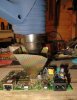
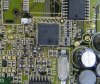
I decided to try to get the AD9865 off the Devolo board and try replace it. This is a 64 pin device in a 9mm square package with a thermal pad underneath. Damn thing won't shift! I made heat guide shaped like a kind of inverted pyramid with the point cut off, out of a bit of baked bean can, so the hollow point fits over the IC, directed the heat gun into the wide opening, watched a whole lot of nothing happening as I blasted hot air in. Tried making nail holes around the bit that fits over the IC, tried again, still no joy.

Tried without the heat-guide, all I managed to do was dislodge a capacitor, took me half an hour to get the damn thing back. Grrrrr.

So, any suggestions how to tackle this? A smd re-work station is out of the question! I need a process I can repeat to solder the new chip in - I do have some solder paste I can use for that.

Thanks :)
 
I took a couple of photos...

Maybe I should make the pyramid thing more so it fits onto the heat gun, and has more vents in the sides? Then more hot air gets to the chip and not blown back over my hand...
 

Attachments

  • mystic-heat-pyramid-thing.JPG
    mystic-heat-pyramid-thing.JPG
    90.1 KB · Views: 359
  • chief-suspect.JPG
    chief-suspect.JPG
    77.4 KB · Views: 347
Last edited:
Actually, just looked on flea-bay. Can get a whole Devolo that works for less than the cost of the modem chip I want to replace. Kind of frustrating...
 
Actually, just looked on flea-bay. Can get a whole Devolo that works for less than the cost of the modem chip I want to replace. Kind of frustrating...
First thought that came to mind was: "It is reasonable to be so". One hour of your time, it is maybe much more than that...

Once you buy the new one, now, free of any pressure you could do it. Who knows?

BTW, I had access a soldering station and a set of tips, some of them very narrow. According to comments of someone who seemed to know what was all this about, the desoldering technique was using that narrow tip? to heat the chip by moving it fast over the terminals in a circular motion until it was loose that you could displace it with a hard tap on the board.

The few I desoldered was in old boards where I was not concerned about damages. It worked. (Cannot recall if any had termal pad).
 
Well, since you know it's bad, the first thing to do is CUT THE PINS. Then remove them one at a time.

With the thermal pad, you might have to heat from the bottom and possibly the top too. EPOXY really doesn't like to conduct heat.

If it was glued in anyway, twisting would release the bond.

My very first SMT solder/desolder was about that size, but no thermal pads.

This was before the ROHS noise. Once the IC was removed and the pads cleaned up and tinned if necessary I used a technique suggested by a friend.

I used 63/37 solder which is basically imperative for SMT stuff of that ERA. The solidus and liqudus points are identical.
So, I tacked the corners AND..

get this. I turned everything UPSIDE DOWN so the chip was above my head and then just dragged solder across the pins. Later, I turned it the right way and removed whatever bridges there was.

In some respect you might be able to get a re-work stencil and re-flow that way.

http://www.google.com/url?sa=t&rct=...ZI4AQ1nmq1k42sw&bvm=bv.74894050,d.cGU&cad=rja

Here http://www.zeph.com/ is an interesting place to hang out to get some ideas.
 
You are on a hiding to nothing unless you apply good flux and gently pre-heat the board around the device from below to just beneath the melting point of the solder. The rework wand merely ramps up the temp to activate the flux and melt the solder on the device pins. The glue dots soften and become elastic at a lower temp, so once the solder is fully liquified, a gentle twist and lift motion is all that's needed to remove it. I know, easier said than done :)

KISS has suggested the only reasonably workable alternative for larger flat packs, but I should point out that it carries the risk of the cutter being pulled down into the board by the remaining pin stubs, which will inevitably result in cut or ripped up tracks and pads. The pads are not so much of a problem to fix usually, but a track running between two pads and disappearing down a via under the device is almost always fatal to the board in my experience.

The hand soldering process KISS suggested is similar to how I was taught to do it when smd work began to become mainstream by an old friend that worked for Pace Europe. He was one of the trainer's that used to visit large factories to show them how to rework equipment using Pace rework tooling. The process uses a small rounded spoon tip to carry a small solder reservoir and, after applying flux, the tip is wiped across the pin/ pad interface in one, deliberate and gentle fluid motion. Each pin will wet and draw just enough solder from the reservoir to form the proper joint web. Using this method took me a fairly long time to get to grips with, but now I rarely have to remove more than 1 or 2 bridges per device :)
 
Hi folks, thanks for the input.

I'm not sure cutting the pins is an option with this package - on the data sheet it's described as a "Lead Frame Chip Scale Package" - the drawing shows the connections being kind of underneath. Have a look at the photo, you can see devices next to it with actual leads - the suspect just has kind of bumps. And when I've de-soldered this one, I have the same problem again, soldering the new one.

"Drag soldering" as I read it's called - I read a good instructable about that - thought I'm not sure it's an option here for the same reason.

I thought about heating from underneath, but I'm very wary of it because of the components underneath - I don't want to unsolder them! I think this (8 layer!) board is giving pretty good heatsinking too - doesn't help. Heatgun is such a blunt instrument.

The datasheet is here: https://www.analog.com/static/imported-files/data_sheets/AD9865.pdf. The package drawing is on page 47. That big thermal pad is the enemy.
 
What I can say is Yikes!

Soldering it back in, you can use this https://www.proto-advantage.com/store/images/PRODUCTS/PA0096-S_0.JPG trimmed and re-flow it.

Is it worth paying someone to replace it? I think the answer was no and this is more of a learning experience.

It almost makes me want to have a milling machine, but even if I did, I'd have to practice.

What it probably suggests is IR heating, such as this: https://www.amazon.com/gp/product/B...d_t=201&pf_rd_p=1535523722&pf_rd_i=B00C17YRLS
 
Yeah, that looks like it would do it! Lot of money I don't have. That's a nifty little mask - is just to spread the paste through?

I'll try making a different sleeve for the heat gun, but thinking it's just going to end up in the scrap box. Breaks my heart.
 
The "mask" is called a solder "stencil". The video on their website show how to use them, I just bought some protoboards from them which have to be modified before use. I have to split the thermal pad mechanically to be able to use it. I haven't done any stencil stuff yet. stencils don't have to be metal. They could be Mylar.
 
Status
Not open for further replies.

Latest threads

Back
Top