JAMES IRVINE
New Member
I was wondering if anyone can tell me if my wiring diagram will work. I'm mainly concerned with the components around the 4069UB, I'm convinced everything to the left of the 4069UB will be fine.
This is a view of a veraboard with the copper tracks having a left/right right/left horizontal arrangement. The capacitor has not been added because I've still to receive the component but it will be placed on the track saying capacitor with both legs on the same track, although may'be that needs to be changed.
Will the capacitor need to have both legs on different tracks?
All lines are just copper track connections to redirect current.
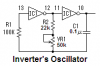
The original circuit diagram is from this link **broken link removed**
**broken link removed**[/url][/IMG]
This is a view of a veraboard with the copper tracks having a left/right right/left horizontal arrangement. The capacitor has not been added because I've still to receive the component but it will be placed on the track saying capacitor with both legs on the same track, although may'be that needs to be changed.
Will the capacitor need to have both legs on different tracks?
All lines are just copper track connections to redirect current.
The original circuit diagram is from this link **broken link removed**
**broken link removed**[/url][/IMG]