Continue to Site

Welcome to our site!

Electro Tech is an online community (with over 170,000 members) who enjoy talking about and building electronic circuits, projects and gadgets. To participate you need to register. Registration is free. Click here to register now.

  • Welcome to our site! Electro Tech is an online community (with over 170,000 members) who enjoy talking about and building electronic circuits, projects and gadgets. To participate you need to register. Registration is free. Click here to register now.

Calculating duty cycle

Status
Not open for further replies.

tbr75

New Member
Hello again,

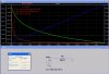
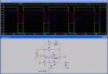
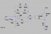
I'm trying to design a circuit that flashes an LED once a second. It needs to have 20% duty cycle. I have attached my circuit, along with the graph.

What I don't know how to do is calculate the resistor and capacitor values to get the correct duty cycle. The negative feedback resistors as well as the capacitor values in the attached schematic give the correct graph, but I don't know why it is that they work. Basically I'm looking for some way to calculate C, Rl, and Rh for certain time constants.

I've tried using τhigh=C(Rh||150k) and τlow=C(Rl||150k). I get the correct value for τhigh (.2 sec) but not for τlow.

Any help is appreciated.
Thanks, Trent

Rh is 200k in the attachment, Rl is 800k.
 

Attachments

  • LTSpice.png
    LTSpice.png
    41.4 KB · Views: 347
  • LtSpicegraph.png
    LtSpicegraph.png
    57.4 KB · Views: 207
You want a PRT (Pulse Repetition Time) of 1 second which is a PRF (Pulse Repetition Frequency) of 1 Hz. You want an on time of 200 mS (20% Duty Cycle). Given those numbers and what you want to do (LED On 200 mS, LED Off 800 mS) I would think about just using a 555 timer circuit running astable with a PRT of 1 second and a 20% duty cycle. You may want to give this a read with a focus on this part:

To achieve a duty cycle of less than 50% a diode can be added in parallel with R2 as shown in the diagram. This bypasses R2 during the charging (mark) part of the cycle so that Tm depends only on R1 and C1:

The 555 can easily directly drive your LED.

Ron
 
Doggy,

I could use some pots, however the school has a very limited selection of pots. I don't believe they have as high of pot values as I need.

Reloadron,

Part of the project requirements is that it must be done with op amp circuitry, more specifically the LM324. As a matter of fact, this circuit can be found on the LM324 datasheet.

I have attached the project requirements.

Thanks for the help, I do agree that a 555 timer would be much easier.
Trent
 

Attachments

  • LEDflasher.doc
    11 KB · Views: 160
increasing the value of the capacitor will decrease the resistance values required

increasing R5 value will increase your off time
increasing R8 value will increase your on time
 
True, I do understand what you're saying. However, I've already done my "fine tuning" through Lt. Spice and I have the correct resistors and capacitor for my high and low time(as shown in the graph) so I don't really have the need for pots. What I'm trying to figure out is how do those values combine to give me my high and low time constants?
 
Hello there tbr75,

The equation for the time period (high or low) is:

t=ln(5/3)*R*C

where R is either R8 or R5 and C is the capacitor C1.

Because you have diodes in the feedback and each resistor works on only one part of the cycle, that equation has to be used twice, once for R8 and once for R5, and the two times have to be added to get the entire time period for one cycle.

This means we have:

t1=ln(5/3)*R8*C1
and
t2=ln(5/3)*R5*C1

and the total time period is:
tp=t1+t2

and that's how the two time periods work together.

Note that in real life the op amp will have a limited output voltage less than the supply voltage. This will mean the times t1 and t2 will be a bit less than the simplified calculation above. With a 5v supply it could be as high as 20 percent less time because the output may be limited to only 3.5 to 4v max.

The way we get the first equation above is by starting with the equation for a charging capacitor and equate that to the two voltages that the other resistors produce with an op amp output of either high or low, then solve for t.
 
Last edited:
Hello there tbr75,

The equation for the time period (high or low) is:

t=ln(5/3)*R*C

where R is either R8 or R5 and C is the capacitor C1.

Because you have diodes in the feedback and each resistor works on only one part of the cycle, that equation has to be used twice, once for R8 and once for R5, and the two times have to be added to get the entire time period for one cycle.

This means we have:

t1=ln(5/3)*R8*C1
and
t2=ln(5/3)*R5*C1

and the total time period is:
tp=t1+t2

and that's how the two time periods work together.

The way we get the first equation above is by starting with the equation for a charging capacitor and equate that to the two voltages that the other resistors produce with an op amp output of either high or low, then solve for t.

That makes sense. Thank you MrAl. However when I plug in the resistor and capacitor values I get t1=.235s and t2=1.175s and tp=1.41s. And the Lt. Spice simulation gives the correct t1 and t2. Any idea why this is?
 
That makes sense. Thank you MrAl. However when I plug in the resistor and capacitor values I get t1=.235s and t2=1.175s and tp=1.41s. And the Lt. Spice simulation gives the correct t1 and t2. Any idea why this is?


Hello again,


Yes. You have to read my previous post again because i added something to it while you were making your reply. It said that the real life times could be lower because the output of the LM324 does not go completely up to +5v, and in fact at 5v it would only go up to around 4v or so. You can verify this with your simulator.
The effects are that the charge time with the output high changes to:
t=ln(625/406)*R*C

and the discharge time will be slightly decreased also:
t=ln(198/125)*R*C

My original post was not meant to be super accurate, only to represent how things in general work. If the output went up to the full 5v then those equations would apply, but it doesnt go that high so we have to modify the equations a little.
 
Last edited:
Hello again,


Yes. You have to read my previous post again because i added something to it while you were making your reply. It said that the real life times could be lower because the output of the LM324 does not go completely up to +5v, and in fact at 5v it would only go up to around 4v or so. You can verify this with your simulator.
The effects are that the charge time with the output high changes to:
t=ln(625/406)*R*C

and the discharge time will be slightly decreased also:
t=ln(198/125)*R*C

My original post was not meant to be super accurate, only to represent how things in general work. If the output went up to the full 5v then those equations would apply, but it doesnt go that high so we have to modify the equations a little.

Hi MrAl,

I have found with this configuration that the input bias and offset currents must be considered when using a general purpose op amp like the LM324. Note the impact this may have on the charge and discharge rate of the capacitor. The typical Ib of the LM324 is ~45nA with an Ios of ~100na, and will yield a lower output frequency that is not easily predictable due to its impact on the capacitors charge rate. A Fet input amp would be the one of choice with an Ib in the pA range, but that is not within the bounds of the OP, of course. Just something to consider.

Cheers
Merv
 
Last edited:
Hi MrAl,

I have found with this configuration that the input bias and offset currents must be considered when using a general purpose op amp like the LM324. Note the impact this may have on the charge and discharge rate of the capacitor. The typical Ib of the LM324 is ~45nA with an Ios of ~100na, and will yield a lower output frequency that is not easily predictable due to its impact on the capacitors charge rate. A Fet input amp would be the one of choice with an Ib in the pA range, but that is not within the bounds of the OP, of course. Just something to consider.

Cheers
Merv

Hello there Merv,

Well, the largest resistor pumps the cap with a min of about 1/800k amps and that divided by 45na yields a factor of about 27, so the bias would be 27 times smaller than the lowest normal charge current. This would result in a change of plus or minus 2 percent of the total time period which i dont think is very significant for this kind of project. On the other hand, the output voltage limitation i was talking about earlier causes a change as much as 40 percent which is very significant so i included that in the second analysis. This was not meant to be a super accurate analysis anyway as the main goal was to show basically how the two times add together to form the total time period.
 
Last edited:
Hello again,


Yes. You have to read my previous post again because i added something to it while you were making your reply. It said that the real life times could be lower because the output of the LM324 does not go completely up to +5v, and in fact at 5v it would only go up to around 4v or so. You can verify this with your simulator.
The effects are that the charge time with the output high changes to:
t=ln(625/406)*R*C

and the discharge time will be slightly decreased also:
t=ln(198/125)*R*C

My original post was not meant to be super accurate, only to represent how things in general work. If the output went up to the full 5v then those equations would apply, but it doesnt go that high so we have to modify the equations a little.

Okay, so I'm guessing you are using this equation: Vc/Vmax = 1-e^(-t/RC). I have tried to figure out how you are getting your values but with no success. I was thinking along the right path as far as realistic outputs before reading your post, but even with that I can't figure it out. For my purposes, 4V is a close enough estimate for the high voltage and 1V is the low voltage.

You say to equate the Capacitor equation to the voltages across the other resistors. So does that mean when calculating the high time I should set Vc equal to the voltage across the 1meg resistor? (which shows as 1.86V peak in Lt. Spice).

Sorry for the questions, but I'd like to know how this works so I know for the future, not just turn in the correct values without knowing how I got there.

Hello again,


Well you dont have to apologize for asking questions, actually i am happy to see that you are interested enough to ask these kinds of questions in the first place.

The basic equation for a capacitor charging, as you know, is:
Vc=Vmax*(1-e^(-t/RC))

and if the output of the op amp went all the way up to the power supply Vmax would be equal to the power supply voltage. This however is for a capacitor that has initial voltage (often written as Vc(0) or Vc0 ) of zero volts. We have to modify that equation a little to allow it to work with a capacitor that already has some voltage across it before we start the charge period, and that comes out to:

Vc=(Vmax-Vc0)*(1-e^(-t/RC))+Vc0

and you'll note that all we did was subtract the initial cap voltage from Vmax before the multiplication, and then after the multiplication we add it back. What this does is it makes the circuit look like the cap has zero voltage across it relative to Vmax with an offset, and then we simply add the offset back after we do the normal calculation.

Ok, so having an equation for the charge time of the capacitor we note we have three variables Vmax , Vc, and Vc0 to find in order to be able to calculate t (the charge time period). Now if the output of the op amp is equal to the supply voltage, then Vmax would equal 5v, and we can do it that way first if you prefer, but the output is actually a bit lower than that because the output of the op amp can not get up to 5v with a 5v power supply and instead it only reaches up to about 4v. That gives us Vmax, so Vmax=4. Now we need to find Vc0. Just before the start of this charge time period the output was low (0v) so the voltage at the non inverting (+) terminal of the op amp was equal to the resistor divider (made up of R2, R3, and R4) voltage with R3 powered by +5v, so the voltage at the (+) terminal comes from R2 in parallel with R4 and R3 as the upper resistor. Mathematically, this is Vin=5*(60)/(160) because R2 in parallel with R4 is 60k and the other resistor R3 is 100k. This means Vin=1.875 and because that is the switchover point the cap voltage must have been 1.875v just before the start of this charge time period. That means now we know Vc0=1.875 and so now we have to calculate Vc, which is the voltage where the op amp will switch states again after the cap charges.
Since the voltage at the output went up to 4v, we now have the resistive divider with two inputs: one is 5v and the other is 4v. The contribution from the 4v supply is 1.000v, and the contribution from the 5v supply is 1.875, so the sum is 2.875v so the voltage we have to charge up to is 2.875v which will be the value of Vc here, so now we know that Vc=2.875.

Now that we have all three voltages, Vc, Vmax, and Vc0, and of course RC=R5*C1, we can solve that equation:
Vc=(Vmax-Vc0)*(1-e^(-t/RC))+Vc0

for t and that is the time period for the output of the op amp when the output is high.


To calculate the output low time period we would do the same thing calculating the resistive divider voltage and finding the unknown variables, but in instead of the charge equation we would use the discharge equation:
Vc=Vc0*e^(-t/RC)

Does that make more sense now?

You may note that we are still not close to exact yet on the charge calculation especially (1 second as compared to a more close estimate of 0.8 seconds) and this is probably because of the input resistance of the spice model that goes from the inverting terminal to the non inverting terminal. My model has 500k+500k=1 Megohm, which is significant when compared to the 800k resistor we are using for the charge period. To get around this we would have to include that input resistance in the equations too which would complicate things a little more. If you wish to do this we can do that next, or you can do an impedance scaling to make that 1 Megohm input resistance look negligible. To do this simply divide all the resistors by 10 and multiply the capacitor value by 10. This would give us for example 80k for the 800k resistor, 20k for the 200k resistor, and 23uf for the 2.3uf cap. The other resistors would change in the same way. Now when we do the calculations above we get a more accurate result because the input resistance does not affect the outcome very much with lower external impedances. Perhaps this is what Merv found out experimentally.

Let me know if you would like to impedance scale this circuit or work on the equations for the time periods including the input resistance.
 
Last edited:
Hello again,


Just a little update since my last post...


I found that the spice simulation yields a high time period of 0.9 seconds very closely and not really 0.8 seconds as thought. That means our calculation is not off as far as we thought, although without considering the input resistance it is still off by 10 to 15 percent or so.

I also found that considering the input resistance the calculated time period (a much more involved calculation now) comes out much closer to the spice simulation time of 0.9 seconds. That leads me to believe that the input resistance should be considered for better accuracy as well as the less than supply voltage output of the op amp. That doesnt mean we can not approximate just to understand better how this circuit basically works though. By looking at it with the output going all the way to +5v and infinite input resistance we still get a good general idea how this circuit works and how the charge and discharge times add together to form the total time period.
 
Mr. Al,

Thanks for your replies. I understand how it works now. Today I built the circuit on a breadboard, and with what you are saying about the input resistance as well as the tolerances on the components (especially the large resistor values), the circuit produced approximately the correct duty cycle but it was nearly 1.5s for the period. I changed some of the resistor/capacitor values around to get it correct. Also, I had to add a pull-up resistor at the output. Otherwise the LED would not completely turn off.

One more question, say I were to connect many LED's to the output. Is there a general rule to follow as far as how many LED's can be ran without another resistor? I think I may have read somewhere that once you get to four LED's in series it's best to add another resistor, but I'm not sure if that applied to only the type of circuit they were analyzing or all circuits.

Again, thanks for all the help.
Trent
 
In your post #4, you included your assignment details. Did you establish the 2V hysteresis within the bounds described before you attempted to calculate the frequency? And in your frequency calculations, did you include the impedance of the diodes you chose? Lastly, could you post a schematic of your current implementation on the breadboard for analysis to satisfy my growing curiosity?

I really didn't want to interrupt your discourse with MrAl further and it should continue, but I have been following this discussion and I'm interested in the topic having employed this basic design in a past project of my own. I'll contain my curiosity to this as a last post on the subject, as is proper methinks.

Cheers,
Merv
 
Hi again Trent and Merv,


Trent:
You are welcome :)
When the LEDs are in series you only need one resistor. If they are in parallel it is best to use one resistor per LED. The resistor is chosen based on the max output voltage and the total sum of all the LED voltages. It sounds though that you may have to run many LEDs so you may have to use parallel series strings.
Note that the real life op amp may not have that kind of input resistance as i did not test for that yet, i only looked at the spice model and that did have the input resistance so that would change the spice results unless we included that in the analysis. If we find out later it's not there in the real life device, we simply leave it out and use the older equations, no problem there as it makes it easier anyway.
Including the input resistor has been interesting so im glad we looked at that too.

Merv:
Thanks for joining in. You had questions about this circuit or more experience with it too?
 
Merv,

I did calculate the 2 volt hysteresis first. The calculations led to R4 being 3/2 of R3. Also, given only a 5v power supply I needed to add a voltage divider, thus the R2 resistor.

My frequency calculations did not include the impedance of the diodes.

Lastly, I am currently not on my computer and cannot post a new schematic and I also do not have my notebook to tell you the specific values of everything. However, I do remember that there was a 10k pull-up resistor added to the output of the op amp. Also, I believe the same resistors with a 1.3u capacitor yielded approximately a 2.05s total period with around 18% duty cycle.

You are more than welcome to continue posting on the topic, as I'm here to learn and more opinions will help me learn more.

MrAl,

That's what I thought about the LED's, just saw a post that confused me. Thanks again. Perhaps I will check the input resistance on the circuit next time I get a chance.

Oh, and one more change I didn't make but should have was the current-limiting resistor before the LED. It should be smaller as I accidentally used Vbe in my outer mesh calculations instead of Vce. Just thought I'd throw that out there.

Trent
 
I did calculate the 2 volt hysteresis first. The calculations led to R4 being 3/2 of R3. Also, given only a 5v power supply I needed to add a voltage divider, thus the R2 resistor.

That would get you close, but what of the calculations required for the project; are those not required to be presented and explained in your writeup? Ones approach to the solution is more important than the accuracy of the solution. The wrong approach with a close answer by accident was always graded down over the correct approach with a wrong answer. Anyone can drop a decimal point, for instance.

Here is a suggestion. Since the voltages at all points in both states are known, to calculate the values quickly, first set R4 at 10k or some other convenient value. Then take the voltage ratios of the drops across R3 & R4 in both states, and average the two ratios for the scalar of R2. That leaves summing the currents of R2 & R4 in one state and dividing that into the drop of R3 in the same state to get its resistance being mindful that the current of R4 reverses in the change of state. Sketching it out and filling in the known voltage drops helps me keep things straight being in my dotage. :confused:

My frequency calculations did not include the impedance of the diodes.

Your configuration of presents a problem with two diodes in the feedback; one for each of the periods t1 & t2. Given the complexity of the dynamic resistance of both diodes in such a low current range, would it not be a good idea to eliminate the one with the lowest average current and the greatest swing in its dynamic resistance range? Doing that allows t1 to be calculated with just the RC components and a swamping effect for the t2 timing with R5 in parallel with R8 and the diode, mitigating the impact greatly.

Now to come up with the timing for t1, the 0.8s period. The capacitance can be selected based on a few factors like the diode impact. Period t1 is 0.8s and lets put the capacitance at 10uf and are the knowns so Rt1 must be determined. The charge on the cap over that period can be determined as (1+Ln t1)*C. here is a start on the equation:

R = X/((1+ln t1)*1e-5)

EDIT: OOPS! :eek:
After checking my math, I discovered a transposition error. However, you should get the idea and the path to follow. Sorry for the posting an error. :eek:

I'll leave X for you to puzzle out. Here's another hint...take a look at the LM555 datasheet and this app. note: https://www.electro-tech-online.com/custompdfs/2011/02/AN-555.pdf

I'll add a few attachments also. One plot will display the plot of a diode's dynamic resistance with the cursor at 1uA to display the issues noted above. The second will of the circuit I came up with just in case I wasn't clear in my explaination with the plot of the circuit with all parameters at less than 1% error. The only the know values are displayed in the schematic. Note the hysteresis and cap charging between the trigger level of 1.5V and the threshold level of 3.5V.
 

Attachments

  • Dynamic Res.jpg
    Dynamic Res.jpg
    172.8 KB · Views: 180
  • SqWav Gen.jpg
    SqWav Gen.jpg
    149.3 KB · Views: 235
Last edited:
That would get you close, but what of the calculations required for the project; are those not required to be presented and explained in your writeup? Ones approach to the solution is more important than the accuracy of the solution. The wrong approach with a close answer by accident was always graded down over the correct approach with a wrong answer. Anyone can drop a decimal point, for instance.

Here is a suggestion. Since the voltages at all points in both states are known, to calculate the values quickly, first set R4 at 10k or some other convenient value. Then take the voltage ratios of the drops across R3 & R4 in both states, and average the two ratios for the scalar of R2. That leaves summing the currents of R2 & R4 in one state and dividing that into the drop of R3 in the same state to get its resistance being mindful that the current of R4 reverses in the change of state. Sketching it out and filling in the known voltage drops helps me keep things straight being in my dotage.

I originally used these equations:

Vtriplow = Vref*R2/(R1+R2) and Vtriphigh = Vref*R2/(R1+R2) + Vcc*R1/(R1+R2)
where R2 is my hysteresis resistor and R1 is the resistor after Vref.

However, I redid my calculations with nodal analysis at the noninverting input and received a hysteresis resistor of 10k and the two resistors in the divider network as 40k. This gives me a perfect 1.5 volt trigger level and 3.5 volt threshold level. But this is with an output of 4 volts at high and 1 volt at low. How are you getting an actual 0 for low output? Does the LM324 not have a limit on it's output voltage of about 1 volts, thus a 4volt high and 1volt low?

My simulation is attached.

Your configuration of presents a problem with two diodes in the feedback; one for each of the periods t1 & t2. Given the complexity of the dynamic resistance of both diodes in such a low current range, would it not be a good idea to eliminate the one with the lowest average current and the greatest swing in its dynamic resistance range? Doing that allows t1 to be calculated with just the RC components and a swamping effect for the t2 timing with R5 in parallel with R8 and the diode, mitigating the impact greatly.

Now to come up with the timing for t1, the 0.8s period. The capacitance can be selected based on a few factors like the diode impact. Period t1 is 0.8s and lets put the capacitance at 10uf and are the knowns so Rt1 must be determined. The charge on the cap over that period can be determined as (1+Ln t1)*C. here is a start on the equation:

R = X/((1+ln t1)*1e-5)

EDIT: OOPS!
After checking my math, I discovered a transposition error. However, you should get the idea and the path to follow. Sorry for the posting an error.

I'll leave X for you to puzzle out. Here's another hint...take a look at the LM555 datasheet and this app. note: **broken link removed**

I'll add a few attachments also. One plot will display the plot of a diode's dynamic resistance with the cursor at 1uA to display the issues noted above. The second will of the circuit I came up with just in case I wasn't clear in my explaination with the plot of the circuit with all parameters at less than 1% error. The only the know values are displayed in the schematic. Note the hysteresis and cap charging between the trigger level of 1.5V and the threshold level of 3.5V.

I'll work on this part after I figure out the hysteresis part. I do understand what you're saying about the diode's impedance, it is definitely effecting my circuit.
 

Attachments

  • LtSpice2.png
    LtSpice2.png
    16.8 KB · Views: 152
  • LtSpicegraph2.png
    LtSpicegraph2.png
    24.5 KB · Views: 223
Last edited:
Status
Not open for further replies.

Latest threads

New Articles From Microcontroller Tips

Back
Top