Hello all!
I've been set an assignment recently to build a working 8088 system. Now I've spent a few hours reading up on the subject and I think I have most of it down.
I'm having a few problems with the 16-key keyboard/display interface unit and the programmable I/O interface.
For the keyboard I'm using a 4x4 key matrix, the output of which is connected to a 8279. The SL pins of this are connected to 2 3-8 decoders ( one of which is fed into the matrix ( pins 0 - 3 ), the other being fed into the LED digit display )
The interface I'm using is the 8255, I've configured this to be :
PA - Input
PB - Output
PC - Output
We've been asked for a 8/in 16/out interface in the brief
My question is to connect these two devices together, am I right in thinking that I will use the output of the 8279 ( PINS OUTB0-3 and OUTA0-3 ) to be the input of the 8255 ( Pins PA0-7 )??
Am I right in thinking that PB and PC ( outputs ) are both connected to the address bus of the CPU.
Also, are the A0 - A7 pins of the 8255 connected to the input of PA0-7?
The NAND gate bit still confuses me though...
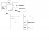
edit:I've made a little picture to try and detail what I want to do. I've left out the 74318 connections for the control lines of the Ram and EPROM, and the memory itself for simplification. I know it's a rough diagram but I hope it's okay.
The brief for the assignment was:
48K Bytes of EPROM for programme memory (choose the components that will give you the exact size of memory).
12K Bytes of RAM for Data memory (choose the components that will give you the exact size of memory).
A Keyboard/Display Interface unit (should support an 8-digit LED display and a keyboard of 16 key switches).
A programmable I/O Port (8 I/P lines and 16 O/P lines, mode 0), Give the right code that will initialise the chip to the required mode.
As you can see I'm still stumped as to the A0 and A1
For the EPROM and RAM I plan to use combinations of 16k, 8k and 4k.as said he wants exact values
Thanks!!
I've been set an assignment recently to build a working 8088 system. Now I've spent a few hours reading up on the subject and I think I have most of it down.
I'm having a few problems with the 16-key keyboard/display interface unit and the programmable I/O interface.
For the keyboard I'm using a 4x4 key matrix, the output of which is connected to a 8279. The SL pins of this are connected to 2 3-8 decoders ( one of which is fed into the matrix ( pins 0 - 3 ), the other being fed into the LED digit display )
The interface I'm using is the 8255, I've configured this to be :
PA - Input
PB - Output
PC - Output
We've been asked for a 8/in 16/out interface in the brief
My question is to connect these two devices together, am I right in thinking that I will use the output of the 8279 ( PINS OUTB0-3 and OUTA0-3 ) to be the input of the 8255 ( Pins PA0-7 )??
Am I right in thinking that PB and PC ( outputs ) are both connected to the address bus of the CPU.
Also, are the A0 - A7 pins of the 8255 connected to the input of PA0-7?
The NAND gate bit still confuses me though...
edit:I've made a little picture to try and detail what I want to do. I've left out the 74318 connections for the control lines of the Ram and EPROM, and the memory itself for simplification. I know it's a rough diagram but I hope it's okay.
The brief for the assignment was:
48K Bytes of EPROM for programme memory (choose the components that will give you the exact size of memory).
12K Bytes of RAM for Data memory (choose the components that will give you the exact size of memory).
A Keyboard/Display Interface unit (should support an 8-digit LED display and a keyboard of 16 key switches).
A programmable I/O Port (8 I/P lines and 16 O/P lines, mode 0), Give the right code that will initialise the chip to the required mode.
As you can see I'm still stumped as to the A0 and A1
For the EPROM and RAM I plan to use combinations of 16k, 8k and 4k.as said he wants exact values
Thanks!!
")
