Can anyone give me some guidance? Please show me some formula, thanks.
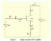
The transistor of Fig.1 has β=99 and a base current of 35μA.
(a) Name the circuit configuration
- COMMON EMITTER CONFIGURATION
(b) Find
(i) IEQ
(ii) Current gain
(iii) Voltage gain
Assuming leakage current is negligible. State also additional assumptions where necessary.
The transistor of Fig.1 has β=99 and a base current of 35μA.
(a) Name the circuit configuration
- COMMON EMITTER CONFIGURATION
(b) Find
(i) IEQ
(ii) Current gain
(iii) Voltage gain
Assuming leakage current is negligible. State also additional assumptions where necessary.
")
