Continue to Site

Welcome to our site!

Electro Tech is an online community (with over 170,000 members) who enjoy talking about and building electronic circuits, projects and gadgets. To participate you need to register. Registration is free. Click here to register now.

  • Welcome to our site! Electro Tech is an online community (with over 170,000 members) who enjoy talking about and building electronic circuits, projects and gadgets. To participate you need to register. Registration is free. Click here to register now.

biasing question

Status
Not open for further replies.

Othello

Member
I am trying to put this amp together and learn something at the same time.

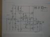
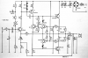
Somehow I don't get this circuit to develop half the supply voltage on the positive side of C9, the output capacitor.
This should be adjustable with P1 but in my case it isn't.

So my question is about the bias of T1.
How does this work, in particular since with C4 at the emitter, how does the DC circuit of the bias look like, I mean C4 blocks all the DC, there is no DC circuit??!!

TIA
Uwe
 

Attachments

  • Amp.JPG
    Amp.JPG
    342.8 KB · Views: 218
Let me see if I understand your question. The amp looks like a single supply amplifier. Usually you see a quasi-complimentary pair for that type of amp, but it has a pnp power bjt on the low side. T1 is the input transistor, with feedback from the output at its emitter. Usually, in a split supply amp, a long tailed differential pair is used, with feedback to the inverting input. Are you asking how this circuit splits the supply voltage?
 
RB is the DC emitter resistor for T1. The current in T! flows through RB and therefore the emitter of T1 is a few volts higher than half the supply voltage, then the output voltage is adjusted with P1.

Is the output voltage higher or lower than half the supply voltage?
Doesn't P1 adjust the voltage?

I fixed your HUGE and dirty schematic and made it a PNG file type.
 

Attachments

  • Amp.png
    Amp.png
    248.8 KB · Views: 185
And I was soo proud of getting the drawing up there at all!!

But thanks, it looks nicer now.


To answer Uncle Scrooges question, the output voltage is higher than the half supply voltage. When I adjust p1 the circuits swings and slowly returns, within a fraction of a volt, to the original voltage.

Supply voltage is 52V and the output wants to be around 30V.
What I don't understand about the bias is where any DC current thru R8 is going to go, I mean it is surrounded by caps.

Uwe
 
Here is the schematic with voltage and current annotations. I have ignored base currents, so the values are approximate, but you can get the gist of it. Note that the 0.27mA through R8 has to flow through T7.
 

Attachments

  • Amp bias.PNG
    Amp bias.PNG
    250.8 KB · Views: 182
Ron H said:
Here is the schematic with voltage and current annotations. I have ignored base currents, so the values are approximate, but you can get the gist of it. Note that the 0.27mA through R8 has to flow through T7.

Ron,

Where did you assume the pot to be set to get the base voltage you did?
 
Analog said:
Ron,

Where did you assume the pot to be set to get the base voltage you did?
The only assumption I made was that the output was at 30V, as indicated by the OP. I worked backwards to the base voltage. I also realized that he won't be able to get the output to go that high with the values of R2, R3, and P1 as shown.
 
Thank you Ron, what service!

Actually I think I was wrong previously, when I said there is no DC path for the current thru R8 (except T7). It could go thru R18, R16 and R14 to ground.

I have this circuit built, though currently without T6 and T7.
I can duplicate all the voltages you indicated except for the one at the base of T7. You indicate 30V and I measure 12V.

This could be the reason that one set of final transistors was destroyed as I experienced sort of a runaway current situation with the voltage drop over the emitter resistors R18, R19 etc. increased quickly. My emitter-base voltage drop on the final transistors is way too high, but I don't know why.

Uwe
 
Ron H said:
The only assumption I made was that the output was at 30V, as indicated by the OP. I worked backwards to the base voltage. I also realized that he won't be able to get the output to go that high with the values of R2, R3, and P1 as shown.

Okay. I used a voltage divider from R2, R3, R4 with P1 set at 5K (midway), and it comes out to 35V at the base of the transistor, that's why I was confused.
 
Pot P2 adjusts the idle current though the output transistors and T3 should be in thermal contact with them to stop thermal runaway. If the idle current is set too high then the output transistors will overheat

The datasheet for the output darlington transistors shows a max base-emitter drop of 2.5V. The base-emitter is just two diodes in series so can't get higher. It would probably be about from 1.4V to 1.8V.
 
I just hooked the amplifier up without the final transistors.
The output voltage was 30V, a bit high given that the supply voltage dropped to 53 V (I hooked the amp up thru a protective resistor to limit the current).

T1 and T2 amplify a sine signal and things don't look too bad.

Then I insert the finals and after a few moments the output voltage slowly starts to decrease while the emitter currents in the finals increase. This continues until the output voltage decreases to about 3V and the emitter current in the finals reach max current allowed by the protective resistor.

I feel like something in the T1 bias isn't stable, but that is only a hunch.

I hope anyone here has better insight.

Uwe
 
Then I insert the finals and after a few moments the output voltage slowly starts to decrease while the emitter currents in the finals increase.
Before you power up the amp, set P2 for minimum resistance so there is little or no idle current in T6 and T7. Then you can gradually turn P2 until the idle current is at the level specified by the design. I would guess somewhere around 50ma or so. It will be a tradeoff between cross-over distortion and power dissipation in T6&7; there will be a point at which increasing the idle current will not decrease distortion.

Then I insert the finals and after a few moments the output voltage slowly starts to decrease while the emitter currents in the finals increase. This continues until the output voltage decreases to about 3V and the emitter current in the finals reach max current allowed by the protective resistor.
I'll bet the voltage after the "protective resistor" also decreased in porportion to the output voltage. You will have to eliminate the resistor once you are confident that the smoke will stay in the transistors before you can fully test it and set the idle current properly.

And don't forget AudioGuru's very important advice:
Pot P2 adjusts the idle current though the output transistors and T3 should be in thermal contact with them to stop thermal runaway. If the idle current is set too high then the output transistors will overheat
 
Last edited:
Well, the amplifier works.

In the end it was a remark by kchriste which lead me to check my power supply (I don't own enough meters to check every point of interest so the behaviour of my power supply was not monitored).

Its strange drop in voltage showed weird things in the amp which I totally misinterpreted.

And also the highlighted, reiterated advice by audioguru may have helped. I tried the amp before it was altogether assembled, assuming that for a last test of a few seconds to minutes the T3 transitor could very well NOT be in thermal contact with the finals. After all the amp would not have time to get warm, no load and all, to make this thermal connection necessary.

And I still don't know what the answer to this is, but now it is all assembled and for the last few hours it works stably and with problems.

Which is nice, now I can build the other 5 amp to complete my electronic crossover-multiamp system.

Thank you

Uwe
 
I forgot to ask something relating to RonH's annotated drawing dated December 11. The small current, 14 mA, going thru T3 must end up at the output, flowing thru the speaker!!

Why is this, I thought the output cap C9 was to prevent any dc reaching the speaker and here suddenly you have dc, up to 2V, connected directly to the speaker!?!?!

Uwe
 
The small current, 14 mA, going thru T3 must end up at the output, flowing thru the speaker!!
Yup, you are correct.
I thought the output cap C9 was to prevent any dc reaching the speaker and here suddenly you have dc, up to 2V, connected directly to the speaker!?!?!
You'll only see the 2.1Vdc at the output (It's accross the 150:eek:
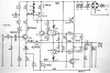
hm: resistor) when there is no speaker attached. With an 8:eek:hm: speaker you should only see 0.1Vdc or so. 14ma through the speaker will not harm it. The reason they do it this way is that it makes for a cheap "bootstrap" for driving the emitter of T7 as close to ground (On the negative peak of the waveform) as possible when the output power is near max.
 
So this amplifier worked for some time on less than the specified voltage until I could get a proper transformer to power the circuit.
Today the transformer arrived and I hooked up the amp to adjust the center rail voltage to half the supply voltage and that worked without a hitch.
After that I tried to adjust the current going thru the power transistors using P2. I started out with P2 in its low resistance postion resulting in a minimal current and then increased the resistance to arrive at about 50 mA, the value specified for this amp.
The setting proves to be unstable, the current slowly increases by itself until I get scared and shut the thing off.

If I stay with a low enough value of P2 I get a stable current, but past a certain value, about 12mA, the current slowly increases and the heat sink also slowly gets very hot!

What is going on? 50 mA thru the power transistors should not make the heat sink too hot to touch, or should it??

Help anybody??

Uwe
 
56V x 12mA= 0.7W which is just enough heat to make the output transistors begin thermal runaway. The heat makes them conduct more current. More current causes more heat.

T3 is supposed to be bolted to the heatsink of the output transistors using thermal grease like they use and be mounted very close to them. The output transistors warm T3 and cause it to also conduct more current. When it conducts more current then it reduces the current in the output transistors.
Then the current in the output transistors should be fairly stable. It might take a few seconds to stabilize.
 
Well, I adjusted the pot to a current of 12 mA and watched the current slowly more than double in 10 minutes. And the heat sink getting very hot.

I was wondering if a faulty thermal connection of the T3 could be responsible, but the power transistors would fail much faster than 10 minutes. So I am baffled.

Uwe
 
56V x 50mA= only 2.8W. This amp needs to have a heatsink that can dissipate about 35W if the speaker is 8 ohms and the amplifier is at full output of about 42W. The heatsink should be barely warm with only 2.8W. Maybe your heatsink is way too small or doesn't have fins that are exposed to free air.
 
I regreased the semiconductors with thermal grease, set P2 to its maximum value and let the amp find its thermal equilibrium. That happenend around 50 mA at which point the heat sink was too hot to touch.

The heat sink in this case is a 1.5" by 1.5" by 6" long alu angle iron, no fins. So the surface area is 18 sqinch. Maybe this is not enough. And yes, all three transistors are bolted to the heat sink in close proximity to each other. When I bring a larger heat sink in thermal contact the temperature goes down and the current thru the finals settles at about 30 mA.

Since 2.8 watt indeed does not seem enough to raise the temperature of the heat sink to "hot", I measured the input current to the amp at the AC stage, 42 volt and 0.5 A. Which leads to the question where is the rest of the power going if of the 21 Watt input power only roughly 10% is dissipated thru the finals??

Uwe
 
Status
Not open for further replies.

Latest threads

New Articles From Microcontroller Tips

Back
Top