Electro Tech is an online community (with over 170,000 members) who enjoy talking about and building electronic circuits, projects and gadgets. To participate you need to register. Registration is free. Click here to register now.
Welcome to our site! Electro Tech is an online community (with over 170,000 members) who enjoy talking about and building electronic circuits, projects and gadgets. To participate you need to register. Registration is free. Click here to register now.
Hi,
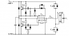
I want to find out how the attached ballast circuit is working. what exactly do the transistors do? what are the Cl and Ch used for and totally I need to know what exaclty every thing is doing.
I'm looking forward to your comments.
The wall outlet is a voltage source.
The tube wants to be driven by a current source.
The circuit converts one to the other.
One is the "dual" of the other.
To differentiate one from the other: I've never seen anything advertised as a power supply or voltage source with a source impedance higher than about 40Ω, so I imagine this circuit has a source impedance of several kΩ.
The transistors alternately switch one end of the fluro tube to the +Vdc rail & the GND rail & are the active part of the oscillator.
The other end of the tube is connected to the junction of 2 Capacitors Cl_Ch which is sortof half Vdc.
The capacitor/inductor values & oscillation frequency are chosen to provide sinusoidal (AC)current to the tube.
This is not an "exactly" explanation but just general.
Have a look at International Rectifier application notes, there are lots of good info on fluro lamp driving.
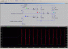
Attached is a simulation of a basic similar circuit except this circuit is not self oscillating.
It is not intended to represent a real fluro inverter circuit but the power stage operating principal is the same.
R1 depicts (Not accurately modelled) a fluro tube.
The frequency here is 20khz supplied by the 2 phase oscillator V1/V2
The light blu trace is the power reference Vm provided by the 2 capacitors (nominal half supply volts)
Purple trace is the current thru R1 which is AC.
Red trace is power switching.
The Vm voltage is actually a result of the current thru each capacitor as the other end of R1 is alternately switched between +V & Gnd by the 2 transistors.
Back to the original circuit (& question):...
The nom. 300Vdc would be from bridge rectified mains(220V) & a filter cap.
Ci bleeds off a bit of the main tube current to heat the filaments, much less filament current once the tube has ionised.
L1,L2,L3 is a base drive transformer for the transistors with L1 & L3 windings 180 deg. phase so each transistor turns on alternately.
L4 smooths the tube current waveform edges (& the C1 & Ch capacitors smooth the top of the current waveform).
The capacitor to GND from the power switching node(Q1-E) supresses transistor turn off oscillations (visible in simulation) & smooths tube current waveform.
The circuit will start by the top transistors turning on (via bleed resistor) & producing current thru L2 winding & this in turn produces base voltage in both L1/L3 windings, turning off Q1 & turning on Q2 & now it will oscillate.
There is very little symmetry in the design of the 2 base drive circuits, this would likely be a result of design testing to optimise the performance.
Fahime, what is your prime need to understand this circuits operation, are you intending to make an electronic ballast for a mains operated fluro.
Fluro inverters that I have played with prototyped have been low voltage 12, 50v although I have tried to & repaired some mains fluro inverters.
Your effort in providing extra information to the OP's problem is well appreciated, especially the fact that you have also included the simulation circuit file so that other people can try for themselves or modify the circuit if they so wish. It also saves time for forum user to re-enter the same circuit again and checked it is exactly the same as posted. It is time wasted for no good purposes.
I hope all other members that post SPICE simulation results would also take the little trouble of providing also the circuit file. The circuit file is a small ASCII text file and only a few KBs long and the RAW file might not even be required.
Fahime, the 2 diodes across the power transistors are for protection. They clamp voltage of the power switching node to the power rails.
Are you going to make a fluro inverter ?
AN1543m.pdf
Thats a good informative Appnote.
I like to Include the sim source files, as you say others can confirm & it is easy to overlook something when providing answers sometimes due to the short time & my rusty-tincan memory.
AN1543 is describing the circuit very well. I'm having some more problems. Please take a look at figure 11 on 6 and answer thesequestions:
1. in the 3th paragraph on page 10,it talks about the influence of C2 and C3. But I can't figure out how!
2. Page 13 talks about the effects of D3 and D2 As well as tonigau said. I need more explanation about it.
3. I still don't know how Cp prepairs the starting voltage. Could u explain its work.
A start is given and the internet and your text books should help you. Once some senior explains, the thrill is gone as perhaps it would amount spoon feeding (if I can use the term)
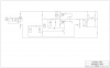
Please take a look at the attached schematic. I have this ballast in hand with some blown components. I figured out what the blown components are but the Q4. Can you guess what it is?
I guess it's a SCR. Am I right?
I have this ballast in hand with some blown components. I figured out what the blown components are but the Q4. Can you guess what it is?
I guess it's a SCR. Am I right?
This site uses cookies to help personalise content, tailor your experience and to keep you logged in if you register.
By continuing to use this site, you are consenting to our use of cookies.