Dr.EM
New Member
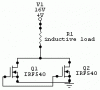
I intend on making a PWM controller for various applications. Occasionally, this may include switching inductive loads, DC motors are a definate possibility. What would be the way to fully protect the 100v max rated MOSFETs (35v max circuit voltage) in the output stage shown (they would be more than 2 in parallel, but I doubt it makes any difference anyhow).
 )
)