Electro Tech is an online community (with over 170,000 members) who enjoy talking about and building electronic circuits, projects and gadgets. To participate you need to register. Registration is free. Click here to register now.
Welcome to our site! Electro Tech is an online community (with over 170,000 members) who enjoy talking about and building electronic circuits, projects and gadgets. To participate you need to register. Registration is free. Click here to register now.
Hi friends!!! This is one of the projects handling by my class as mini project. But unfortunately working of this circuit(analog multiplier) is not getting for us. Please help us in solving it.
I'm gonna assume you didn't design the circuit and that the circuit's designers are correct. So with all the information you gave us, the only thing we can say is "well, if you built it like the schematic then your circuit should work."
We need more information about YOUR circuit and how it's not working as the problems are not with the design of the circuit but the way that it was built.
If We design the circuit, why I ask its working to you?? . It multiplies the voltage E1 and E2 and divides the voltage E3. so, result is E1.E2/E3. It uses the log properties of transistors(most probably gummel plot). we try to simulate it before making the hardware, but again a problem. We use pspice student version and it didn't support for this diagram(no. of nodes are more than its limit).
If you design the circuit and it is not working, then the schematic you give us might be wrong and we might be able to find something. But if the schematic is made by someone else (probably someone professional) then it is probably correct and giving us the schematic won't tell us anything about what might be wrong because the schematic is right, but the circuit was built wrong.
WHether or not the circuit was designed by you, or you're building it from someone else's schematic we need more information.
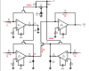
I recognize that as a National Semiconductor schematic.
In a BJT, Ic≈Ie=Is*(e^(Vbe/Vt)-1)), the well-known diode equation.
For Ic>>Is, Ic≈Is*e^(Vbe/Vt)
Ic/Is=e^(Vbe/Vt)
Taking the log of both sides,
Vbe/Vt=ln(Ic/Is)
In the attached schematic,
V(A)=Vbias-Vt*ln(I1/Is)
V(B)=Vbias-Vt*ln(I1/Is)-Vt*ln(I2/Is)
V(C)=Vbias-Vt*ln(I3/Is)
Vbe4=V(C)-V(B)
substituting,
Vbe4=Vbias-Vt*ln(I3/Is)-(Vbias-Vt*ln(I1/Is)-Vt*ln(I2/Is))
simplifying,
Vbe4=Vt*(ln(I1/Is)+ln(I2/Is)-ln(I3/Is))
Vbe4=Vt*ln(I1*I2/(I3*Is))
From the diode equation,
I4≈Is*e^(Vt*ln(I1*I2/(I3*Is))/Vt)
I4/Is=e^ln(I1*I2/(I3*Is)
Taking the log of both sides,
ln(I4/Is)=ln(I1*I2/(I3*Is))
I4=I1*I2/I3
Since R1=R4=R9=R11=10k,
Vout=V1*V2/V3
Q.E.D.
I hope I didn't make any typos.
EDIT: In order for Is to drop out of the equations, all transistors must have equal Is. Therefore, they should all be on the same chip, such as a CA3046. I suspect the asterisks on the schematic refer to a comment in the original app note to this effect.
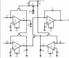
The word "instrumentation" is misleading. An instrumentation amp won't work here. A modern quad op amp would.
I know what you meant, but noobs might not.
I recognize that as a National Semiconductor schematic.
In a BJT, Ic≈Ie=Is*(e^(Vbe/Vt)-1)), the well-known diode equation.
For Ic>>Is, Ic≈Is*e^(Vbe/Vt)
Ic/Is=e^(Vbe/Vt)
Taking the log of both sides,
Vbe/Vt=ln(Ic/Is)
In the attached schematic,
V(A)=Vbias-Vt*ln(I1/Is)
V(B)=Vbias-Vt*ln(I1/Is)-Vt*ln(I2/Is)
V(C)=Vbias-Vt*ln(I3/Is)
Vbe4=V(C)-V(B)
substituting,
Vbe4=Vbias-Vt*ln(I3/Is)-(Vbias-Vt*ln(I1/Is)-Vt*ln(I2/Is))
simplifying,
Vbe4=Vt*(ln(I1/Is)+ln(I2/Is)-ln(I3/Is))
Vbe4=Vt*ln(I1*I2/(I3*Is))
From the diode equation,
I4≈Is*e^(Vt*ln(I1*I2/(I3*Is))/Vt)
I4/Is=e^ln(I1*I2/(I3*Is)
Taking the log of both sides,
ln(I4/Is)=ln(I1*I2/(I3*Is))
I4=I1*I2/I3
This site uses cookies to help personalise content, tailor your experience and to keep you logged in if you register.
By continuing to use this site, you are consenting to our use of cookies.

") . It multiplies the voltage E1 and E2 and divides the voltage E3. so, result is E1.E2/E3. It uses the log properties of transistors(most probably gummel plot). we try to simulate it before making the hardware, but again a problem. We use pspice student version and it didn't support for this diagram(no. of nodes are more than its limit).
. It multiplies the voltage E1 and E2 and divides the voltage E3. so, result is E1.E2/E3. It uses the log properties of transistors(most probably gummel plot). we try to simulate it before making the hardware, but again a problem. We use pspice student version and it didn't support for this diagram(no. of nodes are more than its limit).