Electro Tech is an online community (with over 170,000 members) who enjoy talking about and building electronic circuits, projects and gadgets. To participate you need to register. Registration is free. Click here to register now.
Welcome to our site! Electro Tech is an online community (with over 170,000 members) who enjoy talking about and building electronic circuits, projects and gadgets. To participate you need to register. Registration is free. Click here to register now.
I have just put together my very first amp and would love some feedback on the circuit. The sound quality is disappointing, works ok, is there anything you can think of to improve performance. Thanks!
Q1 will probably be turning completely on and completely off. I suggest that you put a resistor in series with the emitter to make it more linear. That will also make the voltage on the collector of Q1 more less dependent on the gain of Q1, when measured with no signal.
The current flowing through Q2 and Q3 isn't defined. You have the two diodes but you can't be sure that the voltage across them will be exactly the same as the voltage across the base-emitter junctions of Q2 and Q3 that gives the current that you want. I suggest that you put some resistance in series with the emitters of Q2 and Q3, and a larger resistor in series with the diodes.
For example, if the emitters of Q2 and Q3 are at 6 V, you will get about (6-0.7)/680 = 8 mA flowing through R3. If you have 10 Ohms in series, you will get about 0.08 V across the 10 Ohms. With that you could put 1 Ohm in between the emitters of Q2 and Q3, and that will give you about 80 mA flowing through Q2 and Q3.
If the diode voltages are not exactly the same as the base-emitter voltages of Q2 and Q3, that current will vary a bit, but not as much as with your circuit.
You could also add an op-amp to give you feedback, which will improve linearity, but can lead to instability.
I agree with Nigel in as much as a good amplifier will be much more complicated.
Adjustable bias and bootstrapping should help, plus some power decoupling.
With only a single pair of transistors for output and low bias current circuit feeding those, the power will be low.
The output transistor gain is around 50 worst case at moderate power levels (down to 30 or so at high power levels, so the bias current of 10mA or less through R3 will only be able to give about half an amp maximum to the load, at mid voltage.
Without bootstrapping, the current drops as the base voltages increases, so lower and lower output.
Bootstrapping should help; replace R3 with two resistors in series, eg. 2 x 220R, and add a fairly large capacitor from the emitters of the output transistors to the junction of the two resistors - eg. 1000uF.
That keeps the voltage across the lower resistor, to the base of Q2 nearly constant even when the bases are driven near the positive supply, giving more linear output.
A common adjustable output bias circuit uses a small transistor, emitter and collector in place of the two diodes and with a preset pot across it, with wiper top base. Adjusting the wiper adjusts the output bias voltage. Start with it set so the wiper is at the collector end, so minimum bias.
In conjunction with that, you need a low value resistor in series with each output device emitter.
That means the bias current can be adjusted so they are taking a small consistent current all the time, rather than a "hard" changeover from one to the other conducting, causing distortion.
A small standing current in the output devices is what makes it Class AB, rather than Class B.
To get more power at low distortion, you need higher gain in the output devices. The simplest way to mod that would be make them both darlingtons, which would mean the bias control would be at roughly 2.4V
It could also then do with a higher supply voltage.
And, either way, move the bias feed for the input transistor to the output, like the bootstrap cap - and ensure the output voltage is around half supply.
I probably used most of the same parts 2n3904, 2n3906, 2 emitter resistors, two bias resistors, 2 diodes, split supply
and basically put that circuit in a OP-amp feedback loop. I didn't drive a speaker. I drove a solar cell for I-V sweeping.
I just needed +-100 mA. It worked fine.
I made a sweep generator too. Worked at least 25 years and counting probably.
In a later design, I used the LT1010 as a booster stage to isolate capacitance. I almost S$$$ a brick when my circuit would not work on our 1cm^2 solar cells. It worked on the research grade ones. It was used in an I-V converter with mechanically chopped light. There was lots of jitter. I had to put the buffer stage in three places.
Sorry, i now know it is a bad design thanks to your very helpful feedback, it is the first amp i have ever built and I trusted the source, very foolishly so.
Diver3000 and rjenkinsgb can you please write on the circuit diagram i enclosed the resistor values and their location. I want to download the diagram and have it before me as i work on the amp. I am an amateur and want to use the amplifier project to learn and experiment from.
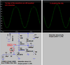
Some of my simulations are missing, maybe on another forum?
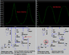
I used similar but different transistors and I show the original circuit with the diodes the correct way then I show much less distortion when the biasing is corrected with R1 and with some negative feedback added. I agree that the distortion will be less and the sensitivity will be higher if my R2 is bootstrapped.
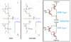
OK, this is my [untested] take on the improvements, a stage at a time:
First, input linearisation and bootstrapping:
(See Stage 1 drawing)
Then DC level adjustment (to set the output at half supply) and make it a proper Class AB amp, with output standing current adjustment:
(See Stage 2 drawing)
Next, if you wish, a higher current gain output stage - converting the single transistors to complementary darlingtons (Szlaki pairs):
(See Stage 3 drawing)
After that, a long tail pair input stage with proper feedback to further improve linearity - but that's going to take a but more thinking about than the mods so far...
----------------------
The variable resistors (presets) will need setting - make sure VR3 has its wiper at the transistor collector end to start with.
Then with power on, monitor the voltage across R8 or R10 and slowly turn the preset until you get just a few millivolts across the resistor.
If the output transistors get hot, you have gone too far!
Then adjust VR2 so the voltage at the output (+ side of C3) is close to half the supply voltage.
That gives the best output voltage "swing" before it starts to distort or clip.
Any comment or improvements welcome.
Edit - drawing errors - see a couple of posts down for the correct ones.
Yes, it was VERY well spotted - it's the sort of thing you look at and your brain sees it how you know it should be, not how it actually is. It's surprising how many commercial circuit diagrams in service manuals have the wrong symbols for one or more transistors.
If you want any proof reading done, AG could be your man!!
Are you trying to say it's not? I made no claims of "hifi" so that's fightin' talk!
Nothing else for it - Soldering irons at dawn
I was planning to put it together at some point to work out the differential amp / long tailed pair stage, as I suspect that will need some ultrasonic rolloff adding to prevent instability.
If I get chance I'll build it tomorrow, to see if it does actually work.
Are you trying to say it's not? I made no claims of "hifi" so that's fightin' talk!
Nothing else for it - Soldering irons at dawn
I was planning to put it together at some point to work out the differential amp / long tailed pair stage, as I suspect that will need some ultrasonic rolloff adding to prevent instability.
After that, a long tail pair input stage with proper feedback to further improve linearity - but that's going to take a but more thinking about than the mods so far...
This site uses cookies to help personalise content, tailor your experience and to keep you logged in if you register.
By continuing to use this site, you are consenting to our use of cookies.