I have attached the data sheet, see page 8.
The muxing is driven at the mains rate, ie. 50 Hz or 60 Hz so one pair of Displays is activated on one half cycle and the other pair on the other half cycle - called "cycle 1 & cycle 2" on the diagram. So far, so good.
But there must be a problem with the labelling of some of the pins in the diagrams. See page 8 for example.
1. Pin 3 is supposedly connected to "10's HR c & HR c" but pin 5 is connected to "HR c & d".
However, "HR c" can't be connected to both pins and since "HR e" is missing, one of the "HR c" must be meant to be "HR e".
2. But there is still a problem even if pin 5 is meant to connect to "HR d & e" since these pins can't be connected together.
3. The same applies to all of the other pins except pins 1, 2, 3, 10 & 14.
For example, pin 4 implies that "HR c" is connected to "HR d". This can't be true.
Does any one know the answer? (I don't have a clock to examine)
I expect that I could probably work it out if I spent enough time on it, but I don't want to "re-invent the wheel" if someone knows the answer.
Any advice will be appreciated
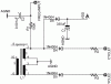
Also note that there is a minor error in the diagram on page 8.
If you number the diodes D1 ~ D4 from top to bottom, the cathode of D2 (shown connected to the junction of the 100 k & the 0.001 uF) is connected to the wrong point.
It should obviously be connected to the other end of the 100 k, ie. to the transformer secondary.
The muxing is driven at the mains rate, ie. 50 Hz or 60 Hz so one pair of Displays is activated on one half cycle and the other pair on the other half cycle - called "cycle 1 & cycle 2" on the diagram. So far, so good.
But there must be a problem with the labelling of some of the pins in the diagrams. See page 8 for example.
1. Pin 3 is supposedly connected to "10's HR c & HR c" but pin 5 is connected to "HR c & d".
However, "HR c" can't be connected to both pins and since "HR e" is missing, one of the "HR c" must be meant to be "HR e".
2. But there is still a problem even if pin 5 is meant to connect to "HR d & e" since these pins can't be connected together.
3. The same applies to all of the other pins except pins 1, 2, 3, 10 & 14.
For example, pin 4 implies that "HR c" is connected to "HR d". This can't be true.
Does any one know the answer? (I don't have a clock to examine)
I expect that I could probably work it out if I spent enough time on it, but I don't want to "re-invent the wheel" if someone knows the answer.
Any advice will be appreciated
Also note that there is a minor error in the diagram on page 8.
If you number the diodes D1 ~ D4 from top to bottom, the cathode of D2 (shown connected to the junction of the 100 k & the 0.001 uF) is connected to the wrong point.
It should obviously be connected to the other end of the 100 k, ie. to the transformer secondary.
Attachments
Last edited: