Please find attached the assignment sheet:
Project 4: Adjustable High Gain / Wideband Feedback Amplifier
1. Introduction.
The aim of this project is to design a versatile amplifier that works in two possible modes: open loop and closed loop modes with different gain and bandwidth requirements.
2. Design
Note that the specifications given below are very similar to a two-stage OPAMP circuitry. While you can definitely benefit from techniques to design two-stage OPAMPs, you don’t need to design any OPAMP. Your design can be both differential or single-ended (i.e. cascading stages of single stage amplifiers).
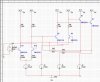
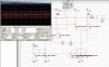
In this project, YOU MAY NOT USE OPAMPS or any other components except, discrete transistors, resistors, capacitors and inductors. A basic block diagram of the amplifier is given in figure 1, and the required specs for both open loop and closed loop mode are given as below:
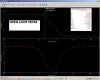
a. Open Loop Mode: High Gain, low bandwidth mode.
- Gain >= 60 dB*
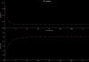
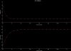
- Bandwidth: DC ‐ 500 Hz
- Supply Voltages: VDD and VSS (these can be anything ranging from 15V to ‐15V)
- Power Consumption < 100 mW
- For no input excitation, your circuit should have an output between VDD/2 to VSS/2.
- Phase Margin > 45°
- Input Resistance > 100KΩ
- Output Resistance: 50 Ω
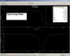
2. Closed Loop Mode: Low Gain, high bandwidth mode.
- Gain >= 20 dB*
- Bandwidth: DC – 100KHz
- Supply Voltages: VDD and VSS (these can be anything ranging from 15V to ‐15V)
- Power Consumption < 100 mW
- For no input excitation, your circuit should have an output between VDD/4 to VSS/4.
- Input Resistance > 100KΩ
- Output Resistance: 50 Ω
*dB (decibel) in magnitude (A) is defined as,
You will switch from open loop to closed loop mode by using a feedback method of your choice (series-series, series-shunt, etc).
3. For Multisim simulation:
- You are required to test your circuit in both open and closed loop modes.
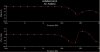
- Your test should be able to resolve the high gain of the open loop mode, phase margin in open loop mode, and input and output resistances accordingly.
I need some pointers regarding the following points:
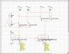
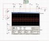
1. How can I find the DC bandwidth so as to satisfy the requirement of 500Hz DC?
2. As I know, the feedback has to usually be from the output to the input. So what and how should we connect in the feedback to get a 100kHz (closed-loop mode)
Project 4: Adjustable High Gain / Wideband Feedback Amplifier
1. Introduction.
The aim of this project is to design a versatile amplifier that works in two possible modes: open loop and closed loop modes with different gain and bandwidth requirements.
2. Design
Note that the specifications given below are very similar to a two-stage OPAMP circuitry. While you can definitely benefit from techniques to design two-stage OPAMPs, you don’t need to design any OPAMP. Your design can be both differential or single-ended (i.e. cascading stages of single stage amplifiers).
In this project, YOU MAY NOT USE OPAMPS or any other components except, discrete transistors, resistors, capacitors and inductors. A basic block diagram of the amplifier is given in figure 1, and the required specs for both open loop and closed loop mode are given as below:
a. Open Loop Mode: High Gain, low bandwidth mode.
- Gain >= 60 dB*
- Bandwidth: DC ‐ 500 Hz
- Supply Voltages: VDD and VSS (these can be anything ranging from 15V to ‐15V)
- Power Consumption < 100 mW
- For no input excitation, your circuit should have an output between VDD/2 to VSS/2.
- Phase Margin > 45°
- Input Resistance > 100KΩ
- Output Resistance: 50 Ω
2. Closed Loop Mode: Low Gain, high bandwidth mode.
- Gain >= 20 dB*
- Bandwidth: DC – 100KHz
- Supply Voltages: VDD and VSS (these can be anything ranging from 15V to ‐15V)
- Power Consumption < 100 mW
- For no input excitation, your circuit should have an output between VDD/4 to VSS/4.
- Input Resistance > 100KΩ
- Output Resistance: 50 Ω
*dB (decibel) in magnitude (A) is defined as,
You will switch from open loop to closed loop mode by using a feedback method of your choice (series-series, series-shunt, etc).
3. For Multisim simulation:
- You are required to test your circuit in both open and closed loop modes.
- Your test should be able to resolve the high gain of the open loop mode, phase margin in open loop mode, and input and output resistances accordingly.
I need some pointers regarding the following points:
1. How can I find the DC bandwidth so as to satisfy the requirement of 500Hz DC?
2. As I know, the feedback has to usually be from the output to the input. So what and how should we connect in the feedback to get a 100kHz (closed-loop mode)
")