Hi and a happy almost new year to everyone,
I have a few questions regarding the ADC acquisition time of the PIC16F family.
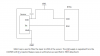
From the Mid-Range Reference Manual,
The TACQ is equal to
Amplifier Settling Time+ Holding Cap Charging time +Temperature Coefficient.
The amplifier Settling Time is given as 5us . What is the amplifier settling time?
Apart from that , the holding cap charge time is given as
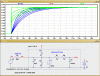
-(All Resistor Elements) * (Cap Value) * ln(1/511)
I understand why R and C needs to be multiplied together. As for ln( 1/511), i assume it's something to do with the 1/2 LSB error used (512 steps for A/D) . However, i don' understand how the concept of how ln(1/511) came about.
The temperature coefficient time on the other hand is given as
(temp-25deg)(0.05us/deg)
What is the reason for calculating the temperature coefficient and how did that formula come about?
Thanks in advance!=)
I have a few questions regarding the ADC acquisition time of the PIC16F family.
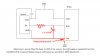
From the Mid-Range Reference Manual,
The TACQ is equal to
Amplifier Settling Time+ Holding Cap Charging time +Temperature Coefficient.
The amplifier Settling Time is given as 5us . What is the amplifier settling time?
Apart from that , the holding cap charge time is given as
-(All Resistor Elements) * (Cap Value) * ln(1/511)
I understand why R and C needs to be multiplied together. As for ln( 1/511), i assume it's something to do with the 1/2 LSB error used (512 steps for A/D) . However, i don' understand how the concept of how ln(1/511) came about.
The temperature coefficient time on the other hand is given as
(temp-25deg)(0.05us/deg)
What is the reason for calculating the temperature coefficient and how did that formula come about?
Thanks in advance!=)
") Thanks alot!
Thanks alot!