Continue to Site

Welcome to our site!

Electro Tech is an online community (with over 170,000 members) who enjoy talking about and building electronic circuits, projects and gadgets. To participate you need to register. Registration is free. Click here to register now.

  • Welcome to our site! Electro Tech is an online community (with over 170,000 members) who enjoy talking about and building electronic circuits, projects and gadgets. To participate you need to register. Registration is free. Click here to register now.

ADC question.

Status
Not open for further replies.

alphadog

Banned
I'm using ADC inside CC2430 MCU.
The ADC present the result (= digital voltage) over 2 bytes - ADCH, ADCL.
(ADCL uses only 6 MSB bits, the 2 LSB bits are always read 0).

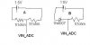
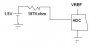
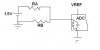
I chose VREF = 3.3V, and entered to ADC a 1.5V battery.
When i chose 12-bit resolution, the ADC showed 15124.
When i chose 7-bits resolution, the ADC showed 15296

Now when i do
[(15124 / 4) / 2^13] * 3.3V = 1.523V
[(15296 / 4) / 2^13] * 3.3V = 1.54V
( the " / 4 " is because ADCL's 2 LSB bits are always read 0).

I have 2 questions please:
1. Did i calculate the analog input correctly?

2. Is there a minimal analog input, that below it the ADC starts being less accurate? how is it in general?

Thank you for any help.
 
hi alpha,
Is the MCU's adc 14bit resolution.?

EDIT:
Looked at the datasheet, its sign + 13bit

Is -Vref = 0?

So the adc count should be, Counts = (Vadc/3.3) * 8192

As you say, a divide by 4 is required.. you could do this by 2 right shifts High and Low registers.
 
Last edited:
Hey Eric,
Thanks for the help :)

1. Regarding (-VREF), there's a problem which i dont understand.
According to datasheet : "For single ended configuration the result is always positive. This is because the result is the difference between ground and input signal which is always possitively signed".
On the other hand, when i short the ADC single-ended input to ground, I receive: 65496, which is a negative number (It must be negative becuase its larger then [(2^13) - 1] which is the largest possitive number the ADC presents over ADCH, ADCL (in 2's complement).
What do you think about it?

2. How do you defined counts?

3. I think i have a mistake, it should be
V_ADC_analog = V_ADC_digital_in_decimal / 4 / (2^13 -1) * 3.3V,
Right?
 
I have another issue please :)

4. It said in the datasheet:
capture-jpg.27222


What does it mean "input resistance, signal"?


5.
capture1-jpg.27223

When i used circuit A, i received V_analog = 0.709V, which is around 5% error so its acceptable.
But when i used circuit B, i recived 0.7V which is weird because it says that the current in the circuit was: (1.5V - 0.7V) / 51 = 15mA, and according to datasheet, VF = 0.7V @ 45mA, which is large error.
What is the problem then with circuit B?
 

Attachments

  • capture.jpg
    capture.jpg
    41.7 KB · Views: 473
  • capture1.jpg
    capture1.jpg
    9.8 KB · Views: 453
Last edited:
hi alpha,

If you are only working with +V input signals, I would set the -Vref to 0V.
Set the +Vref to +3.3V [thats internal.?]

The datasheet says that for 14bit operation the MSBit is the SIGN bit.
So for always positive V input signals this bit will be '0'.

That means the ADCH and ADCL registers will have a maximum count of 8192,
which is 13bit resolution.

The sheet also states that the 'count' [ thats the register value after an A2D conversion has taken place] will be:
ADCH bits 7 to 0 are the highest bits of the 'count' and ADCL has the lowest bits of the 'count'... the ADCL register bits 7 to 2 [6] are the value and the least two bits 1,0 are always '0'.

I would do two right shifts of the count in regs ADCH and ADCL, this will divide the count by 4.
You now have the 'count' normalised [right justified] in ADCH and ADCL.

To convert the 'count to a 'voltage' use this formula:
Vinp[signal] = (3.3V) * (count/8192)

For example: say the count was 4096

Vinp = 3.3V * (4096/8192) = +1.65V

I'll reply to the other questions in a later post.:)
 
I have another issue please :)

4. It said in the datasheet:
What does it mean "input resistance, signal"?

5.
When i used circuit A, i received V_analog = 0.709V, which is around 5% error so its acceptable.
But when i used circuit B, i recived 0.7V which is weird because it says that the current in the circuit was: (1.5V - 0.7V) / 51 = 15mA, and according to datasheet, VF = 0.7V @ 45mA, which is large error.
What is the problem then with circuit B?

hi,
Looking at the datasheet, the 'input resistance' is the equivalent resistance to 0V that the Vsource is connected to.... compare it to a fixed resistor of 197K connected from the adc input pin to 0V.

The reason for specifying the Rinput is to enable you to calculate what effect this resistance will have on your readings.

for example assume that you connected a 1.5V battery via a series resistor to the adc inpout, Let this resistor be say 197K,,, if you now measured with a DVM the voltage on the adc pin it would only be 0.75V...so your adc conversion 'count' would wrong.
It will cause other errors in the readings, due to the charge time/current required by the internal adc cap.

On PIC's it recommended that you keep the resistance of the input signal voltage less than 10K.

Ref the diode circuit which diode are you using.?
 
Last edited:
Thanks a lot Eric!
Here are my replies:

hi alpha,

If you are only working with +V input signals, I would set the -Vref to 0V.

I dont have an option to set (-VREF) in ADC, only to set (VREF).
It is said that for single-ended input pin, the result is always possitive, thats why i was surprised to recevie 65,435 in the the registers (when i shorted ADC input to ground), becasue it represents a negative number in 2's complement representation (It means that the MSB bit in ADCH is '1').
You know why it happend?

Set the +Vref to +3.3V [thats internal.?]
I have a 3.3V that i supply to the MCU with external regulator, and I have an internal 1.25V regulator of MCU which I dont think it uses for any other purpose.
Will it be wrong to use the 1.25V as VREF instead of the 3.3V?

To convert the 'count to a 'voltage' use this formula:
Vinp[signal] = (3.3V) * (count/8192)

For example: say the count was 4096

Vinp = 3.3V * (4096/8192) = +1.65V

I'll reply to the other questions in a later post.:)

Dont you mean 2^(13) - 1 = 8191?


for example assume that you connected a 1.5V battery via a series resistor to the adc inpout, Let this resistor be say 197K,,, if you now measured with a DVM the voltage on the adc pin it would only be 0.75V...so your adc conversion 'count' would wrong.
You mean connection like this:
capture1-jpg.27247

In this case, both the FLUKE and the ADC would show 0.75V.
Why do you say that the FLUKE wont show 0.75V?
(after enough time for its internal cap. to charge, it should show 0.75V).


On PIC's it recommended that you keep the resistance of the input signal voltage less than 10K.
You mean to keep RB less then 10Kohm so it so that RB || Rinternal_adc would be close to RB?
capture2-jpg.27248


Ref the diode circuit which diode are you using.?
I'm using 1N4007 which at VF = 0.7V, its current (by graph) should be 45mA.


Thank you very much :)
 

Attachments

  • capture1.jpg
    capture1.jpg
    6.5 KB · Views: 410
  • capture2.jpg
    capture2.jpg
    7.5 KB · Views: 427
Last edited:
alphadog, you are trying to measure a voltage that is greater than Vref and this is yielding weird results in my opinion.
Try using a voltage divider connected to the battery or Vdd, in order to generate a voltage that is less than Vref.

I am not familiar with your mcu, but I noticed that its ADC has been downgraded to 12-bit. So when you read the results (2 bytes) ignore the two least significant bits. MSB should be 0 in single-ended mode. Then you have a 11-bit value (Vadc) and the analog voltage is Vadc / (2^11 - 1) * 1.25 (alternative formula with 12 bits could be used too)

BTW, the latest datasheet available on TI website is rev 2.1
 
Last edited:
How did you reach 2^11?

15-14-13-12-11-10-9-8-7-6-5-4-3-2-1-0

If you remove bits 15, 1, 0, then you are left with 13 bits unsigned number.
So its V_analig = V_digital / (2^13-1) * VREF.
 
Last edited:
hi alpha.
It is said that for single-ended input pin, the result is always possitive, thats why i was surprised to recevie 65,435 in the the registers (when i shorted ADC input to ground), becasue it represents a negative number in 2's complement representation (It means that the MSB bit in ADCH is '1').
You know why it happend?
What was connected to the ADC input when this occurred.?

I have a 3.3V that i supply to the MCU with external regulator, and I have an internal 1.25V regulator of MCU which I dont think it uses for any other purpose.
Will it be wrong to use the 1.25V as VREF instead of the 3.3V?
No, it wont be wrong to use a 1.25Vref.
The Vref is often chosen to suit the scaling of the input voltage being converted.
eg: if you had a sensor which gave an outout of 0v thru 1.5v, it would logical to use a 1.25Vref.
if the sensor had say an output range of 2.5v, I would use the Vint ref of 2.5v
I'll reply to the other questions in a later post.
Dont you mean 2^(13) - 1 = 8191?
Yes, I have just rounded it up.

In this case, both the FLUKE and the ADC would show 0.75V.
Why do you say that the FLUKE wont show 0.75V?
(after enough time for its internal cap. to charge, it should show 0.75V).
Look at image #1
This is VERY basic diagram, read the PIC 16F series datasheet for a full explanation.

Look at image #2 for the diode, I amke it about ~ 10mA for 0.7V
 

Attachments

  • Image1.png
    Image1.png
    3.7 KB · Views: 131
  • Diode1.gif
    Diode1.gif
    18.1 KB · Views: 146
Last edited:
How did you reach 2^11?

15-14-13-12-11-10-9-8-7-6-5-4-3-2-1-0

If you remove bits 15, 1, 0, then you are left with 13 bits unsigned number.
So its V_analig = V_digital / (2^13-1) * VREF.

The 12-bit value should be stored into bits 15-5

15-14-13-12-11-10-9-8-7-6-5-4-3-2-1-0 (the 12-bit result is highlited)

bit 15 is sign (ignore)

So when the input voltage is equal to Vref, the reading is 11111111111 = 2047 = 2^11-1
 
Last edited:
Thanks Eric :)

hi alpha.

What was connected to the ADC input when this occurred.?
GND was connected to ADC input.
Once I connected a wire from ADC input to GND, and the other time i configurated the ADC input to be the internal GND of MCU.
Received in both a very small negative number.


No, it wont be wrong to use a 1.25Vref.
The Vref is often chosen to suit the scaling of the input voltage being converted.
eg: if you had a sensor which gave an outout of 0v thru 1.5v, it would logical to use a 1.25Vref.
if the sensor had say an output range of 2.5v, I would use the Vint ref of 2.5v

Its good to hear! Thanks. :)


Look at image #1
This is VERY basic diagram, read the PIC 16F series datasheet for a full explanation.
Thank you, I understand it now.
If i have the ADC remained ON even when it doesnt executes conversion, will it solve the problem?


Look at image #2 for the diode, I amke it about ~ 10mA for 0.7V

Thats wierd, could you refer me to datasheet of the 1N4007 you took it from?
Because in the attached PDF it says 0.7V @ 45mA.


Thanks a lot :)
 

Attachments

  • 1n4007.pdf
    68.9 KB · Views: 159
Thank you, I understand it now.
If i have the ADC remained ON even when it doesnt executes conversion, will it solve the problem?

It dosnt really work that way, when you give the MCU a GO command it will do the conversion.

Ref 1N4007 image.
 

Attachments

  • 1N4001a.pdf
    59.7 KB · Views: 211
Last edited:
The 12-bit value should be stored into bits 15-5

15-14-13-12-11-10-9-8-7-6-5-4-3-2-1-0 (the 12-bit result is highlited)

bit 15 is sign (ignore)

So when the input voltage is equal to Vref, the reading is 11111111111 = 2047 = 2^11-1


So you're saying that for 12-bit resolution, bits 3, 2 will always be zero?
Because i checked it now, and when i entered VREF i received (ADCH,ADCL) = 32696, and
32696 = 0111-1111-1010-1000
and as you can see, bit 3 is not zero, so doesnt it mean that bit 3 does play a role ?
 
Last edited:
I see, then i'll decrease the resistance in the circuit.

I really thank you! i learned a lot from you! :)

If you keep the resistance of the voltage source less than 10K it should be OK.

example: say you had a 5V voltage you wanted to convert A2D.

To reduce it to the 3.3V max input you could use say 0.66 ratio resistance divider.
If the bottom resistor was say 6600R then the top resistor would be 3400R, so the input rsesistance would be less than 10K

If you went OTT and made the top one 66K and the botton 34K... thats greater than 10K.. so the conversion could be inaccuarte.
 
Regarding the ADC capacitance,
Is the capacitor being charged only during the conversion?
Meaning when conversions arent being executed, the Vinp that you skected is not connected to the external circuit?
 
Regarding the ADC capacitance,
Is the capacitor being charged only during the conversion?
Meaning when conversions arent being executed, the Vinp that you skected is not connected to the external circuit?

Look at this image, after the conversion is completed the charge on the internal cap leaks away, so read asap after a /GO [ its ready!]
 

Attachments

  • esp02 Mar. 14.gif
    esp02 Mar. 14.gif
    36.3 KB · Views: 132
Status
Not open for further replies.

Latest threads

Back
Top