Continue to Site

Welcome to our site!

Electro Tech is an online community (with over 170,000 members) who enjoy talking about and building electronic circuits, projects and gadgets. To participate you need to register. Registration is free. Click here to register now.

  • Welcome to our site! Electro Tech is an online community (with over 170,000 members) who enjoy talking about and building electronic circuits, projects and gadgets. To participate you need to register. Registration is free. Click here to register now.

Absolute value circuit with opamps

Status
Not open for further replies.

nickagian

Member
Hi!

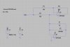
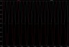
I'm trying to design an absolute value circuit with single supplied opamps. I have read the SBOA068 Application note from TI (available online) and tried to simulate the circuit attached below in LTSpice. This circuit is proposed in the app note from TI in figure 5. Unfortunately, by observing the output waveform (where V(n002) is the output voltage) I presume that some error exists, either in the schematic or my design. As you can see, the output is zero when Vin is positive and an inverted version of Vin, when Vin is negative.

Reading the analysis at the SBOA068 app note it says the following :

1) When Vin < 0, then D1 is forward biased and holds the non-inverting input of U2 at virtual ground. Thus U2 operates as an inverting unity gain amplifier.

(So far, so good. My output follows exactly this description.)

2) When Vin > 0, then D1 is reverse biased and thus has no influence on the circuit. And U2, R1, R2, R3 operate as a voltage follower.

Well, this is not true to me. If D1 is removed from the circuit, I cannot see any voltage follower. The non-inverting input of U2 is again tied to ground and U2 operates again as inverting amplifier. The difference is that the output cannot go negative (due to the single supply operation) and thus the output is zero.

Does anyone know where the error in the schematic is? Or maybe in my thoughts above.
 

Attachments

  • Absolute_value_ci.JPG
    Absolute_value_ci.JPG
    133.9 KB · Views: 709
  • simulation_outpu&#.JPG
    simulation_outpu&#.JPG
    96.9 KB · Views: 490
Last edited:
hi nick,
I have downloaded the app from TI, will you please post the ltspice.asc file so I can check thru it.

This circuit image is the one I use for some projects, it works OK in LTS.

PrecRect2..gif
 
Last edited:
hi nick,

Look at this LTS image, added a 1N914 diode in the top OPA.

AAesp01..gif
 
hi nick,
I have downloaded the app from TI, will you please post the ltspice.asc file so I can check thru it.

This circuit image is the one I use for some projects, it works OK in LTS.

View attachment 39384

Dear ericgibbs,

please find attached the .asc file that I use...

I have also just seen your latest post, so I will try to use the additional diode that you propose and come back.

Regarding the circuit that you use in your projects. Does it work OK with single supply? I assume that no voltage drop due to the diodes is inserted, is that correct?
 
Hi ericgibbs again!

Your suggestion to add this diode at the output of the upper OpAmp was really helpful! Indeed, the circuit is now operating as intended, a full wave rectifier!

Could you please give me additional information? Which of the two circuits is best, according to your opinion? I'm talking between the one published on the app note of TI and the other one that you proposed (with the LM101A), which I assume is from the datasheet of the LM101A.

Thank you very much for your help! You contribution was really important to me!
 
Regarding the circuit that you use in your projects. Does it work OK with single supply? I assume that no voltage drop due to the diodes is inserted, is that correct?

hi,
This is a very basic absolute precision rectifier.
Note: the Vpk out = Vpk in/2

AAesp02..gif
 
hi,
This is a very basic absolute precision rectifier.
Note: the Vpk out = Vpk in/2

View attachment 39386

Yes, I have also considered using this circuit (with also adding an input and an output buffer). But the fact that the pp voltage at the output is half the input voltage, is something that I do not want.
 
Yes, I have also considered using this circuit (with also adding an input and an output buffer). But the fact that the pp voltage at the output is half the input voltage, is something that I do not want.

hi nick,
Your circuit requires a high impedance buffer OPA on the rectified output else the symmetry of the halfwave rectified will be degraded.

AAesp03..gif
 
hi nick,
Your circuit requires a high impedance buffer OPA on the rectified output else the symmetry of the halfwave rectified will be degraded.

View attachment 39387

Hi ericgibbs,

I see...

Actually what I want to do is design an interface of the AC output of an accelerometer to the ADC. Before the rectifier a band-pass filter will be created. The rectified output will then need some peak detection or perhaps low-pass filtering. And afterwards, the signal will be driven to the ADC input.

Where should the buffer be inserted to your opinion? Directly after the rectifier or after the smoothing cap?

hi,
The buffer is shown in my last posted image.
I would add any filtering onto the output of the buffer, keep the full wave rectified signal isolated from any capacitor.

BTW: the CA3140 also comes a dual CA3240 for about 0.5Euro.
 
Status
Not open for further replies.

Latest threads

New Articles From Microcontroller Tips

Back
Top