Electro Tech is an online community (with over 170,000 members) who enjoy talking about and building electronic circuits, projects and gadgets. To participate you need to register. Registration is free. Click here to register now.
Welcome to our site! Electro Tech is an online community (with over 170,000 members) who enjoy talking about and building electronic circuits, projects and gadgets. To participate you need to register. Registration is free. Click here to register now.
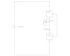
It may be difficult to analyze this without first finding the errors in the diagram. I believe that:
- the package of the 7912 is not identified so it is hard to know if the pinout is correct, however, I think it is incorrect when comparing to the TO-220 version of the this part. I think the intention was that pin 2 be the GND pin, that pin 3 be the INPUT and pin 1 the OUTPUt
- there is no load or output identified which would greatly help identify the purpose of the circuit. As it is shown, the only purpose appears to be to drain some current from the 25VDC supply and perhaps generate a tiny bit of heat.
Some other puzzling things......since there is not enough DC bias voltage to cause both linear regulators to work in their intended way, then either only one of them is holding its output voltage at its rated value, or neither of them is and they are just acting as resistors. The quiescent bias current (through the grnd terminal) of the 7812 is not the same as that of the 7912, so the 7812 will be starved for bias current and not be able to function correctly.
I am confused by this circuit and find that in addition to being poorly drawn (lacking complete part numbers, missing value of R, puzzling symbol for R, incorrect pinouts) that it is either clever for the sake of cleverness (and beyond my understanding) or, more likely, complete nonsense.
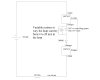
Dear sir, I'm here not to challenge the knowledge or making fool someone but I really need help. Actually this is the part of circuit traced from 4 to 20 mA level transmitter. I've made some observation and rest is traced. Then this circuit is drawn for analyzing and studying the design.
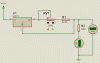
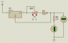
using such an overcomplicated and "overkill" circuit just to make 4 to 20mA is a bit waste of material.
The result is easier to achieve using a single LM317L (low current 100mA) voltage regulator.
Wiring it as a constant current source the feedback resistance is calculated
RF=Uref/Iout, e.g. I out 4mA. Reference voltage is close to 1.25V on all those devices. RF=Uref/Iout=1.25/0.004=312.5Ω. Second calculation includes the maximum desired current which is 20mA RF=Uref/Iout=1.25/0.020=62.5Ω.
You'll find both these values looking at the schematic, RV1 being 250Ω and R1 being 62.5Ω (RV1 + R1 = 312.5Ω).
I don't know the standard values for current to voltage conversion e.g. in building management systems. German standard is a burden resistor of 500Ω, which causes a voltage of 2 to 10V with a 4 to 20mA current loop.
This site uses cookies to help personalise content, tailor your experience and to keep you logged in if you register.
By continuing to use this site, you are consenting to our use of cookies.