Continue to Site

Welcome to our site!

Electro Tech is an online community (with over 170,000 members) who enjoy talking about and building electronic circuits, projects and gadgets. To participate you need to register. Registration is free. Click here to register now.

  • Welcome to our site! Electro Tech is an online community (with over 170,000 members) who enjoy talking about and building electronic circuits, projects and gadgets. To participate you need to register. Registration is free. Click here to register now.

2 phase and single phase PWM

Status
Not open for further replies.
The 1st part of the question 2a) requires the design of a triangle wave generator.

So i need to get values for the capacitor and the 2 resistors (see circuit)
Am I designing them correctly???


R3
R3=5V/0.1mA=50K

C1
C1=T/R3 f=50KHz phase thus T=1/f=20uS


C1=20uS/50K=400pF


R1 & R2
The current in R1 and R2 must be the same

Voltage of pwm output / R1 = current = Voltage at input / R2

5V/R1 = 10V/R2

so R1=10K and R2 = 20 K and current is 500uA
 

Attachments

  • triangle wave generator.jpg
    triangle wave generator.jpg
    58.3 KB · Views: 715
  • q.JPG
    q.JPG
    54.1 KB · Views: 380
Hi there,


Is your solution for C1 or R1 correct? I ask because it looks like you used the time period T which is the full width of the triangle when you really should have used one-half of the width, because the triangle is ramping high for one half the period and ramping low for the other half. Did you take that into consideration? I think you will get a smaller cap value if you keep the 50k resistor (do the calc over again).

You may not have to consider these other little things...
The other thing you may have to think about is if the op amp can output rail to rail, or else you may need a supply voltage that is higher than +5v to run that op amp.
Still yet another thing is the slew rate of the comparator. It will have to be fairly decent for a 20us triangle.
 
Last edited:
Hi there,


Is your solution for C1 or R1 correct? I ask because it looks like you used the time period T which is the full width of the triangle when you really should have used one-half of the width, because the triangle is ramping high for one half the period and ramping low for the other half. Did you take that into consideration? I think you will get a smaller cap value if you keep the 50k resistor (do the calc over again).
.


I did not take that into consideration. I will redo that thanks:).

The complete control circuit is attached below for the 2 phase PWM. Mr Al you said before that:
A little more analysis also shows that R2 must be restricted to values that are above
the value of R1 or else the circuit wont work at all when the max and min input voltages
are sourced from the same power supply as the output of the comparator (as in this
actual application).

However in the circuit above in which I derived values for R1, R2, and C1; R1 has 10V across it and R2 has 5V across it & both resistors have the same current thus R2<R1 when I calculated the values above. Am i doing something wrong in my calculation? is R1 supposed to have 5V across it and R2 have 10V across it so that I get R2>R1?
 

Attachments

  • PWM control.jpg
    PWM control.jpg
    98.1 KB · Views: 374
Last edited:
Hi again,


R2 has to be larger than R1 for at least this one following reason:

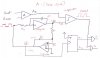
When point B is low it is at -5v, and that means point A is going high heading toward +5v. We will first assume R1=R2 just to illustrate.
Now before point A gets to +5v, we have a negative voltage at point C, which can certainly not trip the comparator output to a high state (which we need to happen for oscillation to occur).
Now once point A finally reaches +5v, that is the maximum it can get to (assuming a perfect rail to rail output integrator), and because R1=R2 that puts exactly 0v at point C, which is still not enough to trip the comparator (assuming even a tiny tiny offset of 1nv). That means that the circuit will never oscillate when R1=R2 unless we get lucky with the offset or the resistors are really slightly different and R2>R1.
Now lets look at the same state when R1>R2.
With R1 larger than R2 the voltage drop across R1 will be greater than across R2, so point C will never be able to get above zero to trip the comparator.
Point C will always remain negative and we're stuck.
Now lets make R2>R1.
With R2>R1, at some point, point A will be high enough to cause a level at point C that is higher than ground (0v) and that will force the output of the comparator high, which is what we need. The output goes high, and that starts the integrator ramping down, and the process repeats only with the polarities reversed.

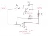
So the conclusions are:
With R1>R2 there will be no oscillation.
With R1=R2 there may be oscillation but only if we get lucky.
With R1<R2 there should be oscillation always, as long as point A can reach a high enough voltage (which may be limited by a real life op amp) or the resistors are sized to work with a lower output.

Numerically, R1=10k and R2=20k look like a good choice because that would allow switching when point A is at either 2.5v or -2.5v which seems comfortable, however you really have to check the particular op amp being used to make sure it's output can get up as high as 2.5v with only a +5v supply, and down to -2.5v with only a -5v supply.
It's also a good idea to check the input ranges for the op amp and comparator to make sure they are within the range of the actual devices used in the real life circuit.
 
Last edited:
Status
Not open for further replies.

Latest threads

New Articles From Microcontroller Tips

Back
Top