Introduction--
Typical bench supplies have both the voltage and current adjustable from essentially zero to their maximum, as well as having meters to display output voltage and current. This usually results in a somewhat complex circuit with numerous active and passive elements.
For example, the ubiquitous LM317 is often used to make a simple supply but its minimum output voltage is nominally 1.25V, requiring an added accurate negative voltage to adjust to a 0V output.
It also requires a separate current-limit circuit if lower than the maximum built-in limit is desired.
And it has a dropout voltage of around 2-3V depending upon the output current, requiring a higher input voltage for a given maximum output voltage, thus increasing dissipation in the regulator and reducing efficiency.
Discussed here is the paper design and simulation of a simple power supply circuit using one LT3081 LDO regulator, 2 transistors, and 9 passive parts (excluding the power source) to perform the voltage control, current control, and current monitor functions, with the added bonus of a regulator-temperature monitor output.
This should be a useful basic design starting point for hobbyists and school labs who want to build a simple, robust bench supply for electronic testing, learn something in the process, and perhaps save some money, depending upon how fancy it's packaged. and how the input power source voltage is generated.
LT3081--
The limitations mentioned in the first two paragraphs are minimized by using the low-dropout (LDO), 1.5A, 36V, LT3081 regulator. Internal protection circuitry includes reverse-battery and reverse-current protection, current limiting and thermal limiting to minimize failure from abuse. Its voltage and current output can be adjusted down to essentially zero with a single pot for each. It can operate in either a constant-voltage or constant-current mode, and has outputs for monitoring its temperature and output current, which can be easily displayed on a meter.
The device is not inexpensive (≈$5 USA) but its simplicity and low parts count in this application means the overall parts and assembly costs will likely be significantly less than using a discrete parts design or cheap IC regulator such as the LM317, with all the associated circuitry required to perform these same functions.
Voltage Output Control--
The LT3081 regulator internal reference generates an accurate 50μA constant-current out of the SET terminal, which is used to generate a voltage across an external control resistor to ground. This voltage at the SET pin is reflected at the regulator output (follower function), thus determining the output voltage.
So, for example, if the control resistor is 100kΩ, the SET (and thus output) voltage will be 50μA x 100kΩ = 5V.
If a pot is used for this control resistor, setting the resistance to zero will thus give zero output voltage.
Current Limit Control--
The LT3081 has a current limit input that allows output current adjustment from zero to maximum with a single pot between the Ilim and OUT terminals.
Current and Temperature Monitor--
The regulator has current and temperature monitor outputs that can be used to display these parameters on a meter, avoiding the need for a current shunt or added temperature sensor.
Simulation Results--
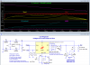
The LTspice simulation of the circuit is shown below:

This shows the current limit varied from zero to maximum by pot U2 (bottom trace), the voltage setting fixed at 15V by pot U4, and the R_Testload resistance varying linearly from 31Ω at the start to 0.1Ω at the end of the simulation time (top trace).
The maximum output, (V(out), yellow trace), goes to very near the lowest voltage of the input ripple, (V(V+), red trace), showing the low dropout of the LT3081 (Vdo = 1.5V maximum @1.5A).
[Input DC voltage is supplied from a 15Vac transformer and a Schottky bridge rectifier which provides about 20Vdc. See Laptop Charger Alternate Input paragraph below for an option to this.]
The maximum output setting is determined by the parallel value of pot U4 and R2.
The values shown have a maximum parallel value of 320kΩ giving a maximum output voltage setting of 320k * 50μA = 16V.
The current limit is determined by the value of pot U2 in parallel with resistor R1 where RILIM = ILIMIT/360mA/kΩ + 450Ω.
With the pot at its minimum, the limit is essentially zero (<1mA simulated).
A linear pot can be used but an audio/logarithmic pot will give finer adjustment at low current levels.
Q1 and Q2 are configured as a current-mirror to generate a load of ≈6mA, which provides the required worst-case minimum load current of 5 mA for the output to remain regulated, as shown here.
 That allows the output to be very near 0V at the zero volt setting (<8mV simulated). Without that, and no other external load, the output would go well above its set value, even at the zero setting.
Q1 and Q2 need to be a matched pair as shown, which are on the same substrate for thermal equilibrium, otherwise thermal runaway can be a problem.
A 75Ω fixed resistor to ground could also be used, which would bring the zero setting output offset to <100mV according to the data sheet, but that would dissipate several watts of power at the highest output voltages.
Heat Sink--
The LT3081 should be ordered with the TO-220 package and mounted on a good heat-sink (possibly with a fan) since its dissipation can go over 20W under low output voltage, high current conditions.
Note that the TO-220 tab is electrically connected to the OUT pin so the heat sink must be isolated from the circuit and ground.
Wiring--
To minimize output voltage drop from ground resistance, use a separate wire to make the ground connection for R2 and U2 directly at the supply's output banana terminal, separate from the current carrying ground wire.
Unfortunately there's no way to compensate for the positive output wire resistance so use a large wire (e.g. 18 gauge) from the LT3081 output to the banana terminal.
Current Limit Note--
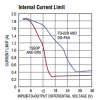
For safe-area protection of the internal power transistor, the LT3081 has an internal maximum current limit that depends upon the input-to-output voltage difference as shown below.
Thus, for example, the current with the output shorted to ground will be about 1.2A with this circuit's nominal 20Vdc input for a TO-220 package.
This can be seen in the simulation maximum current (green) trace on the right side where there is a wiggle in the trace as the limit current is reduced due to the R_TestLoad reaching a low enough resistance value that the increase in Vin-Vout is sufficient to cause the internal current limit to kick in.

Power Transformer--
It's not well known but the transformer current rating must be derated to about 60% when it is used to generate a DC current with a rectifier-filter. This is because the large current spikes from charging the large filter capacitor (C1) at the peak of the AC waveform generate high RMS power in the transformer primary and secondary winding resistances.
So for 1.5A DC output, the transformer should have a current rating of at least 1.5/0.6 =2.5Arms to avoid overheating.
Laptop Charger Alternate Input--
Instead of a transformer-rectifier-capacitor to power the supply, a 19-20V, ≥30W laptop charger can be used, which are often available cheaply in thrift shops. They are small, have high efficiency, and would allow a slightly higher output from the supply of about 18V-19V (with a suitable increase in the value of R2), since those supplies generally have low output ripple.
Some universal laptop chargers go up to 24Vdc (example) which would allow a maximum output of about 22-23V.
But note that an increase in the input supply voltage will proportionally increase the dissipation in the Lt3081 for a given output current and voltage.
Monitor Output Useage --
The LT3081 has two current outputs that can be used to monitor the device internal temperate and the value of the output load current (avoiding having to add a current shunt or temperature sensor to measure these parameters).
The scaling for these outputs is 1μA/°C for temperature and 200μA/A for current. These currents can be converted to a voltage to drive a panel meter or go to a microprocessor analog (A/D) input. The conversion is readily achieved by adding a 1% resistor selected to give the desired output voltage (1V full-scale maximum) from each of the outputs to ground.
The basic current monitor accuracy is about 10%, which should be sufficient for most bench uses. If desired it could be calibrated with an external ammeter, using a pot for the current scaling resistor.
Of course these two measurements can share one meter using a SPDT switch to select the desired measurement at the meter input.
Alternately the temperature monitor output can be connected to a comparator to light a panel LED and give a warning when the device temperature becomes too high.
Increasing Output Voltage--
The LT3018 input voltage can be increased to the maximum recommended value of 36V, giving a maximum output voltage of over 34V.
Of course the regulator power dissipation goes up accordingly so the heat sinking and power handling capability of the regulator must accommodate that.
Increasing Output Current--
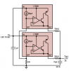
If more than 1.5A output is desired, two (or more) LT3018 devices can be simply paralleled as shown below.

This maintains the current limit and thermal protection built into the devices.
It also allows the Imon (current monitor) outputs to be summed into one resistor to ground to indicate the total output current by a voltage (1V maximum as previously noted).
A variable current limit control will require a multiple-gang pot (one gang for each regulator) so that all will be limited to approximately the same current.
Their temperature outputs will have to be monitored separately if that information is wanted.
The indicated 10mΩ output balancing resistors can be provided on a PCB by short pieces of narrow copper trace as detailed in the LT3081 data sheet. If built on a vector type board, 2" of 28 gauge or 4.5" of 24 gauge copper wire has a resistance of about 10mΩ.
Typical bench supplies have both the voltage and current adjustable from essentially zero to their maximum, as well as having meters to display output voltage and current. This usually results in a somewhat complex circuit with numerous active and passive elements.
For example, the ubiquitous LM317 is often used to make a simple supply but its minimum output voltage is nominally 1.25V, requiring an added accurate negative voltage to adjust to a 0V output.
It also requires a separate current-limit circuit if lower than the maximum built-in limit is desired.
And it has a dropout voltage of around 2-3V depending upon the output current, requiring a higher input voltage for a given maximum output voltage, thus increasing dissipation in the regulator and reducing efficiency.
Discussed here is the paper design and simulation of a simple power supply circuit using one LT3081 LDO regulator, 2 transistors, and 9 passive parts (excluding the power source) to perform the voltage control, current control, and current monitor functions, with the added bonus of a regulator-temperature monitor output.
This should be a useful basic design starting point for hobbyists and school labs who want to build a simple, robust bench supply for electronic testing, learn something in the process, and perhaps save some money, depending upon how fancy it's packaged. and how the input power source voltage is generated.
LT3081--
The limitations mentioned in the first two paragraphs are minimized by using the low-dropout (LDO), 1.5A, 36V, LT3081 regulator. Internal protection circuitry includes reverse-battery and reverse-current protection, current limiting and thermal limiting to minimize failure from abuse. Its voltage and current output can be adjusted down to essentially zero with a single pot for each. It can operate in either a constant-voltage or constant-current mode, and has outputs for monitoring its temperature and output current, which can be easily displayed on a meter.
The device is not inexpensive (≈$5 USA) but its simplicity and low parts count in this application means the overall parts and assembly costs will likely be significantly less than using a discrete parts design or cheap IC regulator such as the LM317, with all the associated circuitry required to perform these same functions.
Voltage Output Control--
The LT3081 regulator internal reference generates an accurate 50μA constant-current out of the SET terminal, which is used to generate a voltage across an external control resistor to ground. This voltage at the SET pin is reflected at the regulator output (follower function), thus determining the output voltage.
So, for example, if the control resistor is 100kΩ, the SET (and thus output) voltage will be 50μA x 100kΩ = 5V.
If a pot is used for this control resistor, setting the resistance to zero will thus give zero output voltage.
Current Limit Control--
The LT3081 has a current limit input that allows output current adjustment from zero to maximum with a single pot between the Ilim and OUT terminals.
Current and Temperature Monitor--
The regulator has current and temperature monitor outputs that can be used to display these parameters on a meter, avoiding the need for a current shunt or added temperature sensor.
Simulation Results--
The LTspice simulation of the circuit is shown below:
This shows the current limit varied from zero to maximum by pot U2 (bottom trace), the voltage setting fixed at 15V by pot U4, and the R_Testload resistance varying linearly from 31Ω at the start to 0.1Ω at the end of the simulation time (top trace).
The maximum output, (V(out), yellow trace), goes to very near the lowest voltage of the input ripple, (V(V+), red trace), showing the low dropout of the LT3081 (Vdo = 1.5V maximum @1.5A).
[Input DC voltage is supplied from a 15Vac transformer and a Schottky bridge rectifier which provides about 20Vdc. See Laptop Charger Alternate Input paragraph below for an option to this.]
The maximum output setting is determined by the parallel value of pot U4 and R2.
The values shown have a maximum parallel value of 320kΩ giving a maximum output voltage setting of 320k * 50μA = 16V.
The current limit is determined by the value of pot U2 in parallel with resistor R1 where RILIM = ILIMIT/360mA/kΩ + 450Ω.
With the pot at its minimum, the limit is essentially zero (<1mA simulated).
A linear pot can be used but an audio/logarithmic pot will give finer adjustment at low current levels.
Q1 and Q2 are configured as a current-mirror to generate a load of ≈6mA, which provides the required worst-case minimum load current of 5 mA for the output to remain regulated, as shown here.
Q1 and Q2 need to be a matched pair as shown, which are on the same substrate for thermal equilibrium, otherwise thermal runaway can be a problem.
A 75Ω fixed resistor to ground could also be used, which would bring the zero setting output offset to <100mV according to the data sheet, but that would dissipate several watts of power at the highest output voltages.
Heat Sink--
The LT3081 should be ordered with the TO-220 package and mounted on a good heat-sink (possibly with a fan) since its dissipation can go over 20W under low output voltage, high current conditions.
Note that the TO-220 tab is electrically connected to the OUT pin so the heat sink must be isolated from the circuit and ground.
Wiring--
To minimize output voltage drop from ground resistance, use a separate wire to make the ground connection for R2 and U2 directly at the supply's output banana terminal, separate from the current carrying ground wire.
Unfortunately there's no way to compensate for the positive output wire resistance so use a large wire (e.g. 18 gauge) from the LT3081 output to the banana terminal.
Current Limit Note--
For safe-area protection of the internal power transistor, the LT3081 has an internal maximum current limit that depends upon the input-to-output voltage difference as shown below.
Thus, for example, the current with the output shorted to ground will be about 1.2A with this circuit's nominal 20Vdc input for a TO-220 package.
This can be seen in the simulation maximum current (green) trace on the right side where there is a wiggle in the trace as the limit current is reduced due to the R_TestLoad reaching a low enough resistance value that the increase in Vin-Vout is sufficient to cause the internal current limit to kick in.
Power Transformer--
It's not well known but the transformer current rating must be derated to about 60% when it is used to generate a DC current with a rectifier-filter. This is because the large current spikes from charging the large filter capacitor (C1) at the peak of the AC waveform generate high RMS power in the transformer primary and secondary winding resistances.
So for 1.5A DC output, the transformer should have a current rating of at least 1.5/0.6 =2.5Arms to avoid overheating.
Laptop Charger Alternate Input--
Instead of a transformer-rectifier-capacitor to power the supply, a 19-20V, ≥30W laptop charger can be used, which are often available cheaply in thrift shops. They are small, have high efficiency, and would allow a slightly higher output from the supply of about 18V-19V (with a suitable increase in the value of R2), since those supplies generally have low output ripple.
Some universal laptop chargers go up to 24Vdc (example) which would allow a maximum output of about 22-23V.
But note that an increase in the input supply voltage will proportionally increase the dissipation in the Lt3081 for a given output current and voltage.
Monitor Output Useage --
The LT3081 has two current outputs that can be used to monitor the device internal temperate and the value of the output load current (avoiding having to add a current shunt or temperature sensor to measure these parameters).
The scaling for these outputs is 1μA/°C for temperature and 200μA/A for current. These currents can be converted to a voltage to drive a panel meter or go to a microprocessor analog (A/D) input. The conversion is readily achieved by adding a 1% resistor selected to give the desired output voltage (1V full-scale maximum) from each of the outputs to ground.
The basic current monitor accuracy is about 10%, which should be sufficient for most bench uses. If desired it could be calibrated with an external ammeter, using a pot for the current scaling resistor.
Of course these two measurements can share one meter using a SPDT switch to select the desired measurement at the meter input.
Alternately the temperature monitor output can be connected to a comparator to light a panel LED and give a warning when the device temperature becomes too high.
Increasing Output Voltage--
The LT3018 input voltage can be increased to the maximum recommended value of 36V, giving a maximum output voltage of over 34V.
Of course the regulator power dissipation goes up accordingly so the heat sinking and power handling capability of the regulator must accommodate that.
Increasing Output Current--
If more than 1.5A output is desired, two (or more) LT3018 devices can be simply paralleled as shown below.
This maintains the current limit and thermal protection built into the devices.
It also allows the Imon (current monitor) outputs to be summed into one resistor to ground to indicate the total output current by a voltage (1V maximum as previously noted).
A variable current limit control will require a multiple-gang pot (one gang for each regulator) so that all will be limited to approximately the same current.
Their temperature outputs will have to be monitored separately if that information is wanted.
The indicated 10mΩ output balancing resistors can be provided on a PCB by short pieces of narrow copper trace as detailed in the LT3081 data sheet. If built on a vector type board, 2" of 28 gauge or 4.5" of 24 gauge copper wire has a resistance of about 10mΩ.