The lowest input to output voltage drop you can get with a standard bridge rectifier is at least a volt through the 2 conducting diodes for each half cycle, even with Schottky diodes in the bridge (other than for low current levels).
That can cause a dissipation of a watt per amp or more of output current in the bridge diodes and require a heat sink at higher current levels.
In contrast, a MOSFET bridge circuit can have a very low voltage drop as determined by the ON resistance of the selected MOSFETs, thus a bridge drop of less than a 100 millivolts can be achieved using common, low on-resistance MOSFETs, even for relatively high output currents.
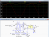
The LTspice simulation of such a circuit is shown below for a typical filament transformer AC output voltage of 6.3Vrms. as might be used for a 5V linear regulated supply.
That's an application where the extra volt or so gained by the MOSFET bridge over a Schottky bridge is significant compared to the magnitude of the output voltage and helps relax the output filter and/or regulator dropout voltage requirements.
This allows the use of a common LM317 for the 5V regulation while still maintaining its required 2V dropout overhead, for example.
The circuit certainly is more complex than a simple diode bridge, requiring an added comparator IC chip and six resistors, but may be worth it if you need maximum output voltage and efficiency from a low voltage, bridge rectifier circuit, especially at higher current levels.
Being able to avoid a bridge heat sink for higher current levels may be a sufficient reason to use the circuit, even if you don't otherwise need the efficiency.

V_Tran simulates a transformer floating output.
The bridge consists of two N-MOSFETs and two P-MOSFETs.
The MOSFETs actually conduct in their reverse direction and block in the forward direction, which works because MOSFETs conduct equally well in both directions when ON (they can't block in their reverse direction due to their intrinsic substrate diodes).
Thus the N-Channel MOSFET gates of M1 and M3 are simply connected to the bridge opposite side of the AC input to turn them ON for the proper time to conduct in the reverse direction for each half cycle, and OFF otherwise.
The same type of gate connections could be made for the P-MOSFETs with a resistive output load, such as a DC motor, but that doesn't work with the filter capacitor output of a typical bridge rectifier DC supply circuit.
The problem is, the bi-conduction characteristic of the MOSFETs when ON, means that the P-MOSFETs will conduct in the forward direction if the MOSFET is biased ON (bridge reverse direction) after the peak voltage is reached, and thus discharge the capacitor.
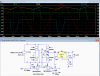
To prevent that, there are two comparators to control the gates of the P-MOSFETs, M2 and M4 respectively, and turn them ON only when the capacitor is charging, to avoid any back current discharge of the capacitor.
The comparator determines the point of the respective sine-wave node where the voltage goes slightly negative with respect to ground.
Thus U1 turns on M2 during the positive peak at node 1 and U2 turns on M4 during the positive peak at node 2.
This negative voltage (due to the N-MOSFET ON resistance) means the N-MOSFET in the sensed line is starting to conduct in its reverse direction through the ground connection, indicating the capacitor is starting to charge (which initially occurs through the P-MOSFET substrate diode).
The comparator then turns on the appropriate P-MOSFET (comparator open-collector output pulls gate to ground).
As soon as this voltage turns positive, indicating the peak AC voltage is below the capacitor voltage and it's starting to discharge, the comparator turns the MOSFET OFF (open-collector output turns off, allowing the gate-source resistor to pull the Vgs to zero volts) and stays OFF until the voltage again starts to go negative during the next cycle.
[Note that neither sinewave node voltage goes significantly below ground (equal to the N-MOSFET drop from the current flow), since they are clamped to ground by the N-MOSFETs.]
R6 and R7 add about 7mV of positive offset at the comparator inputs to insure that they turn off after the capacitor stops charging.
For a different input voltage, the value of R4 and R5 should be changed in direct proportion to this change, to keep the offset voltage ≈7mV.
During startup, before there is any output supply voltage to power the comparators and the P-MOSFETs are OFF, the filter capacitor is charged through the P-MOSFETs intrinsic substrate diodes.
The simulation shows the MOSFETs are working properly since the output peak voltage is only ≈30mV below the peak sine voltage, as can be seen in the expanded second plot down.
The MOSFETs need to be logic-level type if the peak AC voltage is below 10V
The MOSFET's ON resistance should be selected for the maximum current you want from the bridge and the maximum voltage drop and dissipation you can tolerate.
There are dual and quad MOSFET packages with one/two N-MOSFETs and one/two P-MOSFETs in a single package that can be used to reduce the parts count.
To calculate the average MOSFET power dissipation, you need to use a MOSFET current value about double the average DC output current because of the high peak currents through the MOSFET (since power is proportional to the square of the current, high peak currents significantly increase the power dissipation over the value calculated using the average current value).
Generally it's desirable to keep the MOSFET dissipation below the point where you need a heatsink.
It should also have a maximum Vds rating of at least 150% of the peak AC voltage.
The maximum peak voltage of the circuit shown is determined by the Vgs limit of the MOSFET's, which is typically 20V peak.
To work above that voltage you would need to add some sort of voltage clamp to limit Vgs to below the selected MOSFET's Vgs rating.
The other limit is the maximum operating voltage of the selected comparator.
If you want an output voltage above that, you will need to a add a simple voltage regulator for the comparator power and limit the output voltage to its maximum.
The LM339/LM393 comparator will operate from a supply and output voltage of 2V to 36V.
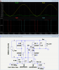
Below is a simulation of the circuit with an LM317 regulator adjusted for a 5V output, with a 1.25A load current.
The simulated transformer is a typical filament transformer with a 6.3Vrms output @ 2.5Arms current and 15% regulation (no load to full load). This is the normal 50% current derating used for a rectifier capacitor-filter load of 1.25Adc from a transformer. The reason for this derating can be seen in the simulation transformer high current peaks which cause the RMS current value to be nearly twice the average (DC) current value.
This gives a calculated transformer series resistance of 0.38Ω and an open circuit voltage of 7.25Vrms as used in the simulation.
With this, the minimum voltage between the the bridge output, V(out), and the LM317 output, V(V+) is about 2.4V for the filter capacitor value shown, which is normally sufficient to avoid dropout of the LM317.

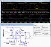
Since the transformer output is floating, you can simply reverse the Out and Gnd connections everywhere in the circuit to give a negative output with respect to Gnd, as shown below:

A caveat is that the circuit has only been simulated, not built by me, so there's always the possibility that the real circuit won't quite work as the simulation shows, but I have good confidence that it will be close enough to be acceptable, since it's a fairly simple circuit.
One possible issue might be the output of the comparators oscillating during their switching time transition.
If so, adding a small amount of hysteresis, such as with a 10MΩ resistor between each output and the positive input, should help.
If you build this, I would like to know how it worked for you.")
In the interest of full disclosure it should be noted that Linear Technology makes the dedicated LT4320 chip that controls four MOSFETs to form a bridge rectifier.
It has the advantage of using four N-MOSFETs rather than two N-MOSFETs and two P-MOSFETs as the subject circuit does..
Another is this chip from Microsemi, which contains two MOSFET 1A bridges.
My circuit was designed primarily for hobbyists who want to use a commonly available IC to control the MOSFETs, and might not have ready access to these somewhat pricey, specialized ones.
That can cause a dissipation of a watt per amp or more of output current in the bridge diodes and require a heat sink at higher current levels.
In contrast, a MOSFET bridge circuit can have a very low voltage drop as determined by the ON resistance of the selected MOSFETs, thus a bridge drop of less than a 100 millivolts can be achieved using common, low on-resistance MOSFETs, even for relatively high output currents.
The LTspice simulation of such a circuit is shown below for a typical filament transformer AC output voltage of 6.3Vrms. as might be used for a 5V linear regulated supply.
That's an application where the extra volt or so gained by the MOSFET bridge over a Schottky bridge is significant compared to the magnitude of the output voltage and helps relax the output filter and/or regulator dropout voltage requirements.
This allows the use of a common LM317 for the 5V regulation while still maintaining its required 2V dropout overhead, for example.
The circuit certainly is more complex than a simple diode bridge, requiring an added comparator IC chip and six resistors, but may be worth it if you need maximum output voltage and efficiency from a low voltage, bridge rectifier circuit, especially at higher current levels.
Being able to avoid a bridge heat sink for higher current levels may be a sufficient reason to use the circuit, even if you don't otherwise need the efficiency.
V_Tran simulates a transformer floating output.
The bridge consists of two N-MOSFETs and two P-MOSFETs.
The MOSFETs actually conduct in their reverse direction and block in the forward direction, which works because MOSFETs conduct equally well in both directions when ON (they can't block in their reverse direction due to their intrinsic substrate diodes).
Thus the N-Channel MOSFET gates of M1 and M3 are simply connected to the bridge opposite side of the AC input to turn them ON for the proper time to conduct in the reverse direction for each half cycle, and OFF otherwise.
The same type of gate connections could be made for the P-MOSFETs with a resistive output load, such as a DC motor, but that doesn't work with the filter capacitor output of a typical bridge rectifier DC supply circuit.
The problem is, the bi-conduction characteristic of the MOSFETs when ON, means that the P-MOSFETs will conduct in the forward direction if the MOSFET is biased ON (bridge reverse direction) after the peak voltage is reached, and thus discharge the capacitor.
To prevent that, there are two comparators to control the gates of the P-MOSFETs, M2 and M4 respectively, and turn them ON only when the capacitor is charging, to avoid any back current discharge of the capacitor.
The comparator determines the point of the respective sine-wave node where the voltage goes slightly negative with respect to ground.
Thus U1 turns on M2 during the positive peak at node 1 and U2 turns on M4 during the positive peak at node 2.
This negative voltage (due to the N-MOSFET ON resistance) means the N-MOSFET in the sensed line is starting to conduct in its reverse direction through the ground connection, indicating the capacitor is starting to charge (which initially occurs through the P-MOSFET substrate diode).
The comparator then turns on the appropriate P-MOSFET (comparator open-collector output pulls gate to ground).
As soon as this voltage turns positive, indicating the peak AC voltage is below the capacitor voltage and it's starting to discharge, the comparator turns the MOSFET OFF (open-collector output turns off, allowing the gate-source resistor to pull the Vgs to zero volts) and stays OFF until the voltage again starts to go negative during the next cycle.
[Note that neither sinewave node voltage goes significantly below ground (equal to the N-MOSFET drop from the current flow), since they are clamped to ground by the N-MOSFETs.]
R6 and R7 add about 7mV of positive offset at the comparator inputs to insure that they turn off after the capacitor stops charging.
For a different input voltage, the value of R4 and R5 should be changed in direct proportion to this change, to keep the offset voltage ≈7mV.
During startup, before there is any output supply voltage to power the comparators and the P-MOSFETs are OFF, the filter capacitor is charged through the P-MOSFETs intrinsic substrate diodes.
The simulation shows the MOSFETs are working properly since the output peak voltage is only ≈30mV below the peak sine voltage, as can be seen in the expanded second plot down.
The MOSFETs need to be logic-level type if the peak AC voltage is below 10V
The MOSFET's ON resistance should be selected for the maximum current you want from the bridge and the maximum voltage drop and dissipation you can tolerate.
There are dual and quad MOSFET packages with one/two N-MOSFETs and one/two P-MOSFETs in a single package that can be used to reduce the parts count.
To calculate the average MOSFET power dissipation, you need to use a MOSFET current value about double the average DC output current because of the high peak currents through the MOSFET (since power is proportional to the square of the current, high peak currents significantly increase the power dissipation over the value calculated using the average current value).
Generally it's desirable to keep the MOSFET dissipation below the point where you need a heatsink.
It should also have a maximum Vds rating of at least 150% of the peak AC voltage.
The maximum peak voltage of the circuit shown is determined by the Vgs limit of the MOSFET's, which is typically 20V peak.
To work above that voltage you would need to add some sort of voltage clamp to limit Vgs to below the selected MOSFET's Vgs rating.
The other limit is the maximum operating voltage of the selected comparator.
If you want an output voltage above that, you will need to a add a simple voltage regulator for the comparator power and limit the output voltage to its maximum.
The LM339/LM393 comparator will operate from a supply and output voltage of 2V to 36V.
Below is a simulation of the circuit with an LM317 regulator adjusted for a 5V output, with a 1.25A load current.
The simulated transformer is a typical filament transformer with a 6.3Vrms output @ 2.5Arms current and 15% regulation (no load to full load). This is the normal 50% current derating used for a rectifier capacitor-filter load of 1.25Adc from a transformer. The reason for this derating can be seen in the simulation transformer high current peaks which cause the RMS current value to be nearly twice the average (DC) current value.
This gives a calculated transformer series resistance of 0.38Ω and an open circuit voltage of 7.25Vrms as used in the simulation.
With this, the minimum voltage between the the bridge output, V(out), and the LM317 output, V(V+) is about 2.4V for the filter capacitor value shown, which is normally sufficient to avoid dropout of the LM317.
Since the transformer output is floating, you can simply reverse the Out and Gnd connections everywhere in the circuit to give a negative output with respect to Gnd, as shown below:
A caveat is that the circuit has only been simulated, not built by me, so there's always the possibility that the real circuit won't quite work as the simulation shows, but I have good confidence that it will be close enough to be acceptable, since it's a fairly simple circuit.
One possible issue might be the output of the comparators oscillating during their switching time transition.
If so, adding a small amount of hysteresis, such as with a 10MΩ resistor between each output and the positive input, should help.
If you build this, I would like to know how it worked for you.
In the interest of full disclosure it should be noted that Linear Technology makes the dedicated LT4320 chip that controls four MOSFETs to form a bridge rectifier.
It has the advantage of using four N-MOSFETs rather than two N-MOSFETs and two P-MOSFETs as the subject circuit does..
Another is this chip from Microsemi, which contains two MOSFET 1A bridges.
My circuit was designed primarily for hobbyists who want to use a commonly available IC to control the MOSFETs, and might not have ready access to these somewhat pricey, specialized ones.
-
 upload_2017-2-1_21-47-34.png
 -
 upload_2017-2-1_22-9-27.png
 -
 upload_2017-2-1_22-24-53.png
 -
 upload_2017-10-9_20-44-13.png
 -
Bridge Rectifier MOSFET Cap Output.asc
